Nguyen Vincent
-
First iteration: testing the hardware
02/20/2023 at 21:17 • 0 commentsAfter verifying that there were no shorts on the PCB (there weren't any, fortunately), I needed to tackle one of the hardest part of the project: the firmware.
The keyboard uses the ZMK firmware, a wireless-first firmware based of the open-source RTOS Zephyr. It's a fairly new firmware, with very talented developers and a blooming community.
As the microcontroller doesn't come with any bootloader, I had to compile and flash one myself to the MCU. For this, I used the Adafruit nRF52 UF2 bootloader. After creating my own board definition and compiling the bootloader .hex file in linux, the bootloader can simply be flashed to the board via its SWD header with a J-link.
Configuring the firmware is then pretty straightforward. Definining switch matrix, row-column transform, enabling DC-DC buck converter, crystals, merging PRs, setting up github actions, ... I won't get into too much detail here as it will get boring, but the takeaway is that most of the functions were working as intended.
However, after testing the firmware and assembling the board, I could detect a few mistakes on the board:
- I forgot to connect some traces to the dual-channel MOSFET for the user LEDs. Not critical but this means that I couldn't have any visual indicator when the board was in bootloader mode.
- Clearance for some of the cables was too narrow.
- Some components were too power-hungry, such as the LDO.
- The e-paper display presented a very noisy image when exposed to direct light.
- I forgot to place the 5.1k pulldown on the inner-side USB connector, which made it impossible to charge the battery when connected to a power bank (charging through the outer-side USB worked though).
- Forgot to enable via tenting.
![]()
-
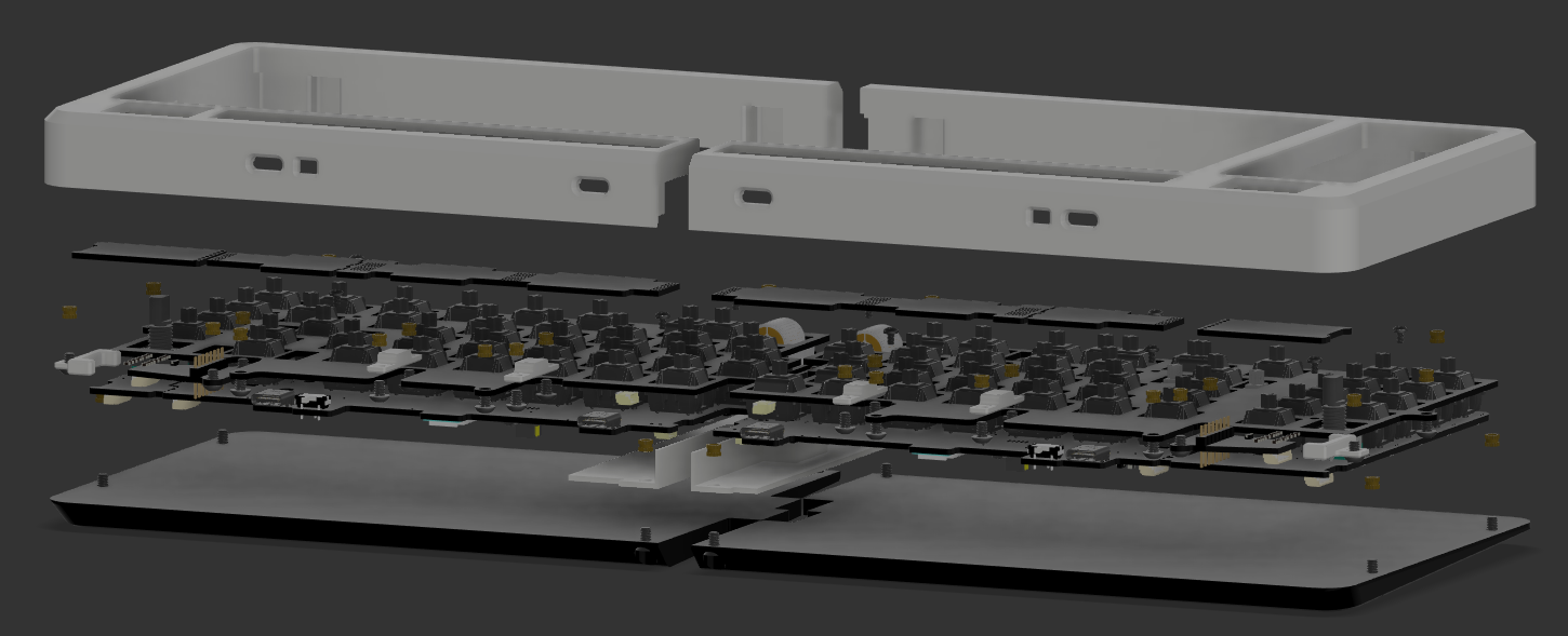
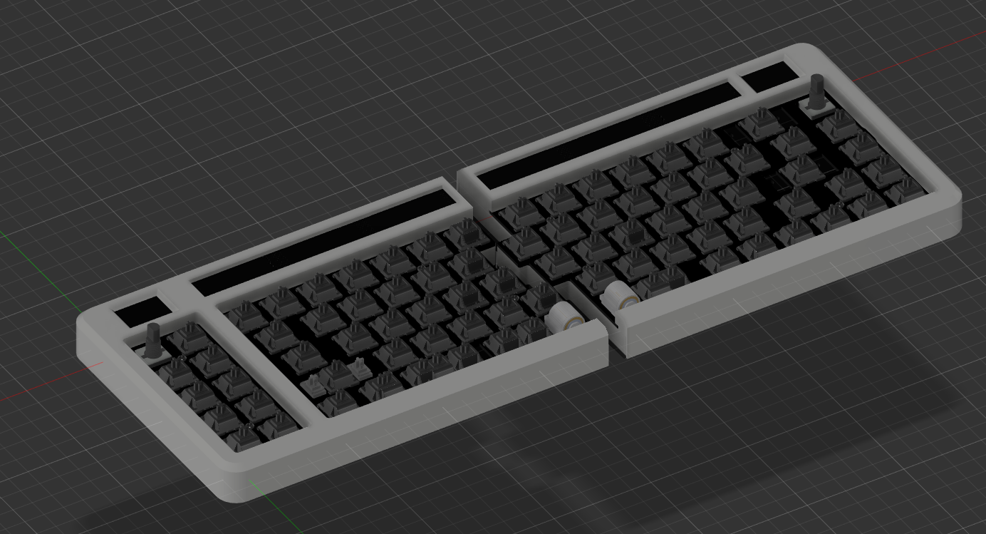
Designing the case for the first iteration
02/20/2023 at 21:03 • 0 commentsThe whole case was designed in Fusion360. The biggest challenge was to get all sub-PCBs to fit inside the case while having no visible screws from the top. The pictures here were taken when designing the first iteration, but more details are given in the project log of when the second iteration was designed.
![]()
![]()
-
Assembling the first iteration
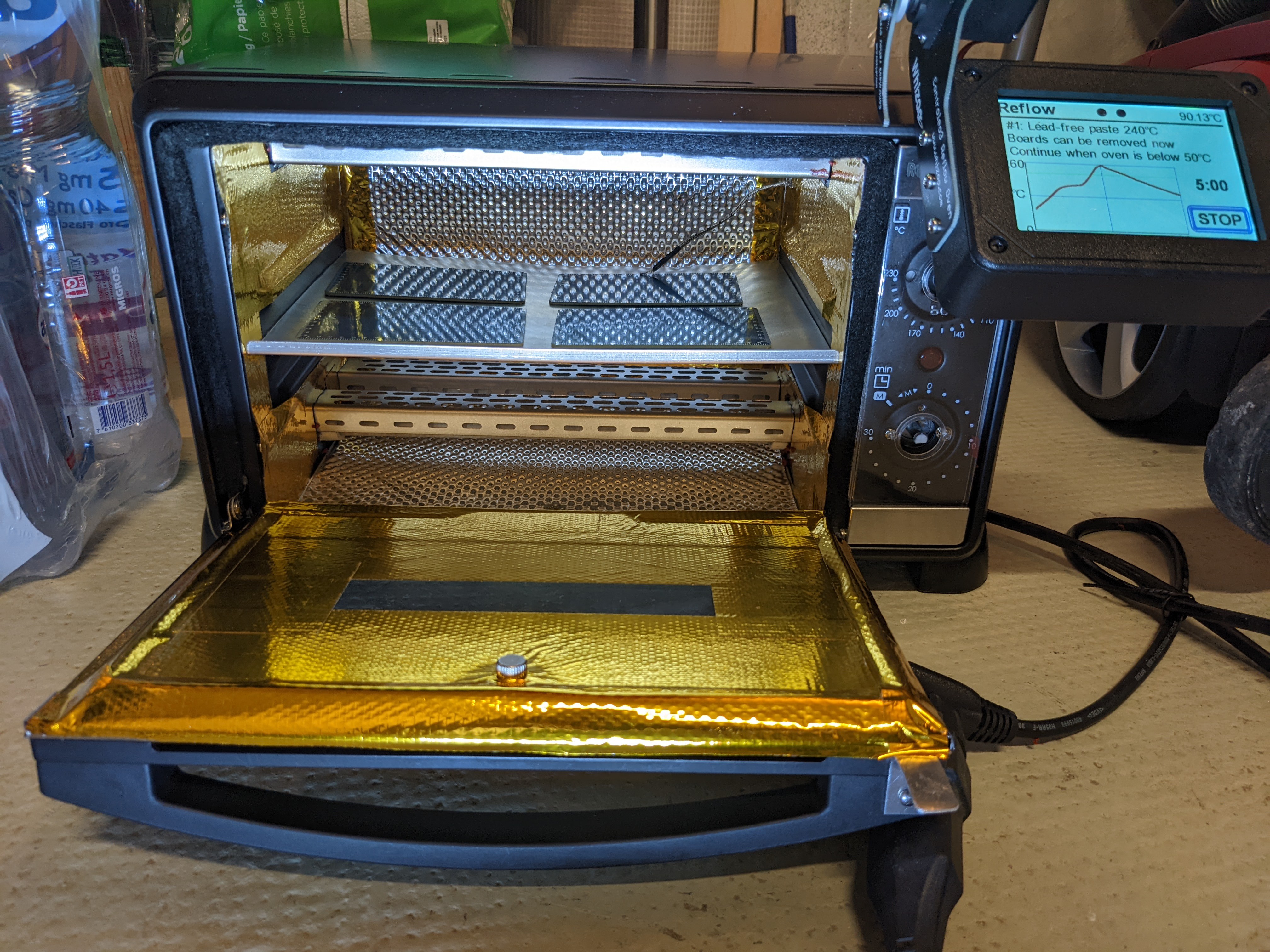
02/20/2023 at 20:59 • 0 commentsAs this was the first iteration of the board, I wanted to keep the costs down as much as possible. My choice of parts made it very expensive to have a one-off assembled by a PCB manufacturer. Fortunately, I have built previously a DIY reflow oven based off the Controleo 3 reflow oven controller. This oven is quite small, which means that it cannot fit a normal TKL sized keyboard, but is perfect for split keyboards :). If you are based in Europe however, it's quite of a pain to build, as there aren't many high-power, small, quartz heater based toasters. Actually, I needed to buy 2 ovens (and burnt one in the process) so I could transfer some of the quartz heaters for larger heating capacity.
You can see in the oven some of the alignment PCBs that I've ordered along with the first iteration of the board. They are useful not only to fix the board in place when aligning the stencil, but also to reduce thermal mass inside the oven during reflow.
![]()
I actually first tested the oven with the external connector boards, with different pastes to see how it affected the result:
![]()
The top one uses lead-free solder paste in a jar, whereas the bottom ones use solder in a syringe. It is clear that the one in a jar gives better results, maybe because I mixed it for a few minutes before applying.
For all PCBs I used JLCPCB as it offered high quality PCBs for half the price of other competitors such as AISLER or PCBWay. This first iteration has a HASL surface finish to reduce cost as it was just to test the overall function. The stencils were ordered with electropolish finish, which reduces failure when applying solder paste by a lot (which is especially important for the nRF52 module, as all of the pads are at the bottom, and very small).
For this iteration, only the left half of the keyboard was assembled (in the picture the PCB is upside down).
Before reflow:
![]()
After reflow:
![]()
Inspecting the PCB (sorry for the messy desk ^^'):
![]()
The components were placed with foot pedal operated vacuum tweezers (Quick 381A). I can't recommend it enough if you often do SMT soldering.
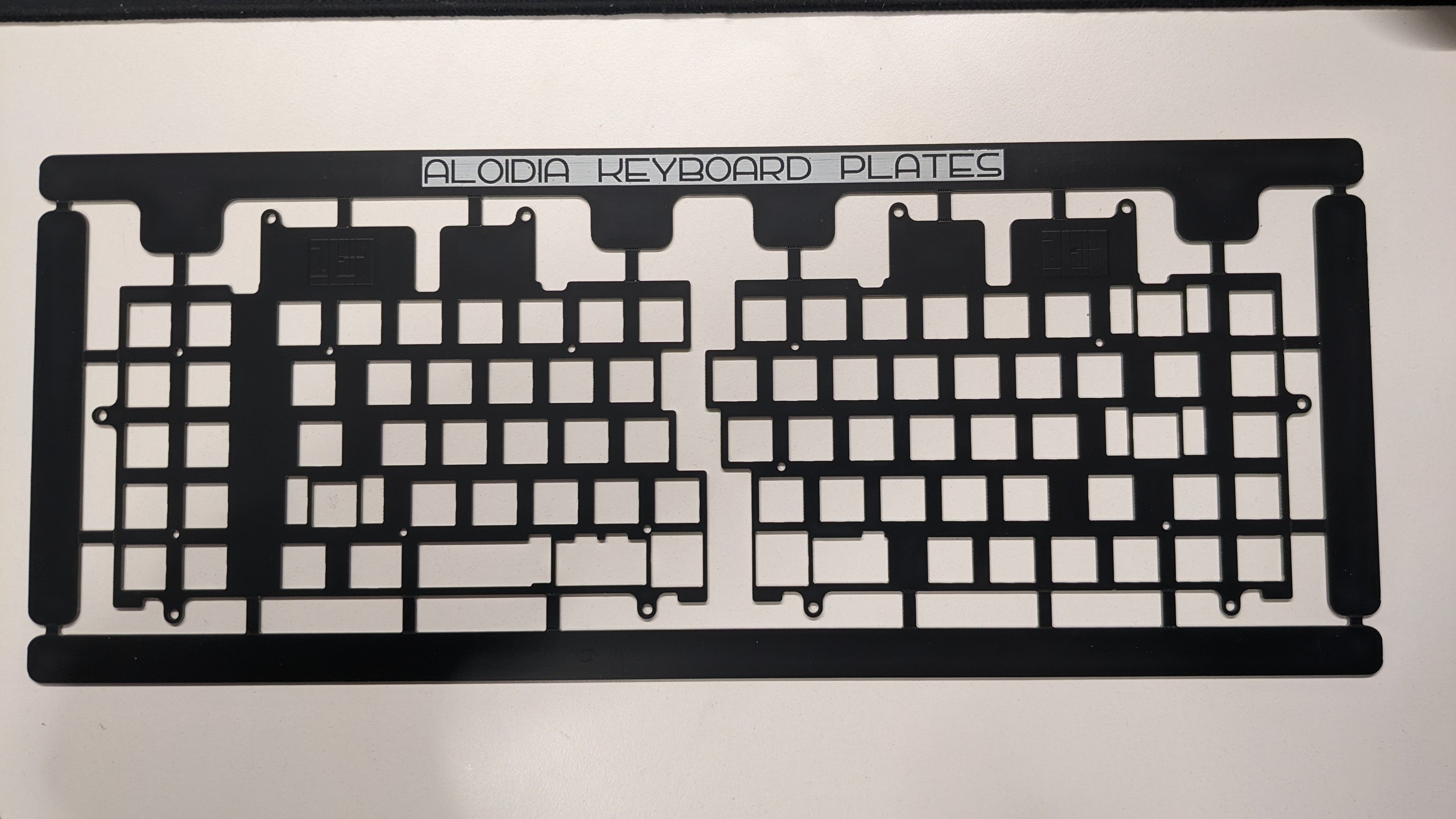
A very neat trick when designing keyboard is that the plate can also be ordered with the PCB (FR4 plate). After designing part of the case, the plate outline can be converted to dxf format and imported in PCBNew. For this project, I've designed plates with custom cutouts and a small tented copper text with the keyboard logo
![]()
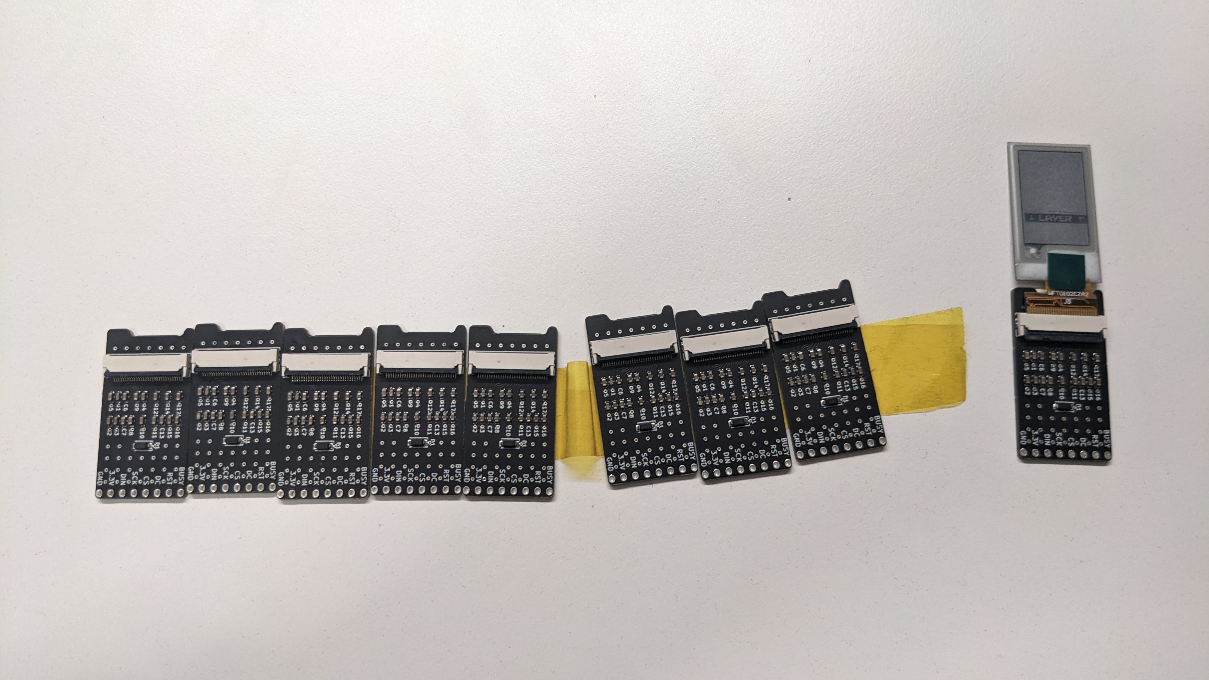
For the e-paper display, I had the PCBs assembled by JLCPCB, as the components that I wanted were only available on LCSC. Being in Europe, shipping components from LCSC was more expensive than just having it assembled.
![]()
-
Aloidia 1.0 rev1
02/20/2023 at 20:28 • 0 commentsThis first prototype was designed with the following specifications
- 65% layout (with additional macro keys or F-keys on the left side).
- PCB can be broken off to reduce it to a 60% layout.
- Designed around the nRF52840 MCU to be compatible with the ZMK firmware.
- Can support 3 solar panels per half.
- Optional rotary encoders on the top corners of each half.
- Optional hotswappable 5-way navigation switch/ mx switch / horizontal rotary encoder near the thumb
- Compatible with e-ink paper display.
- Reliable protection circuit.
- Battery monitoring.
- Two USB port per half to allow for charging both halves at the same time by connecting one to the computer and the two halves together.
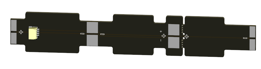
To meet these specifications, 6 different PCBs were designed.
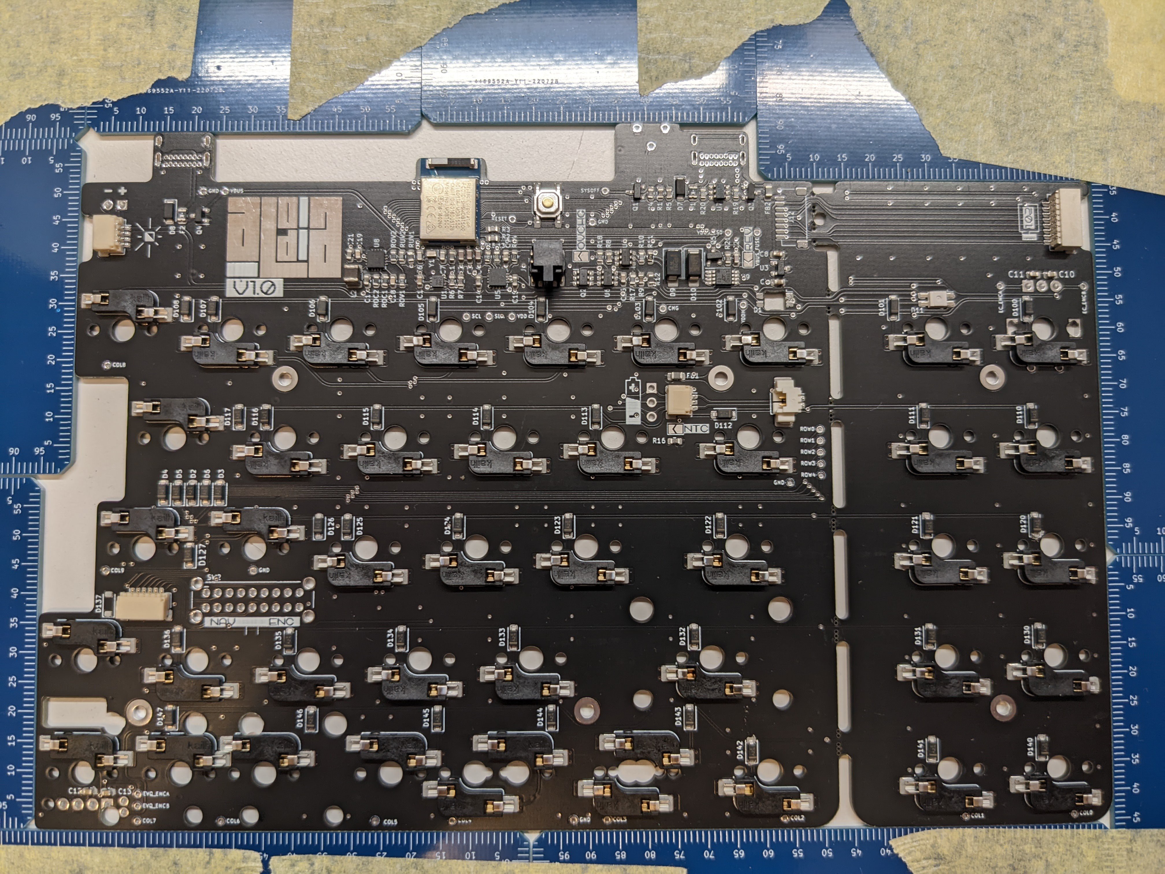
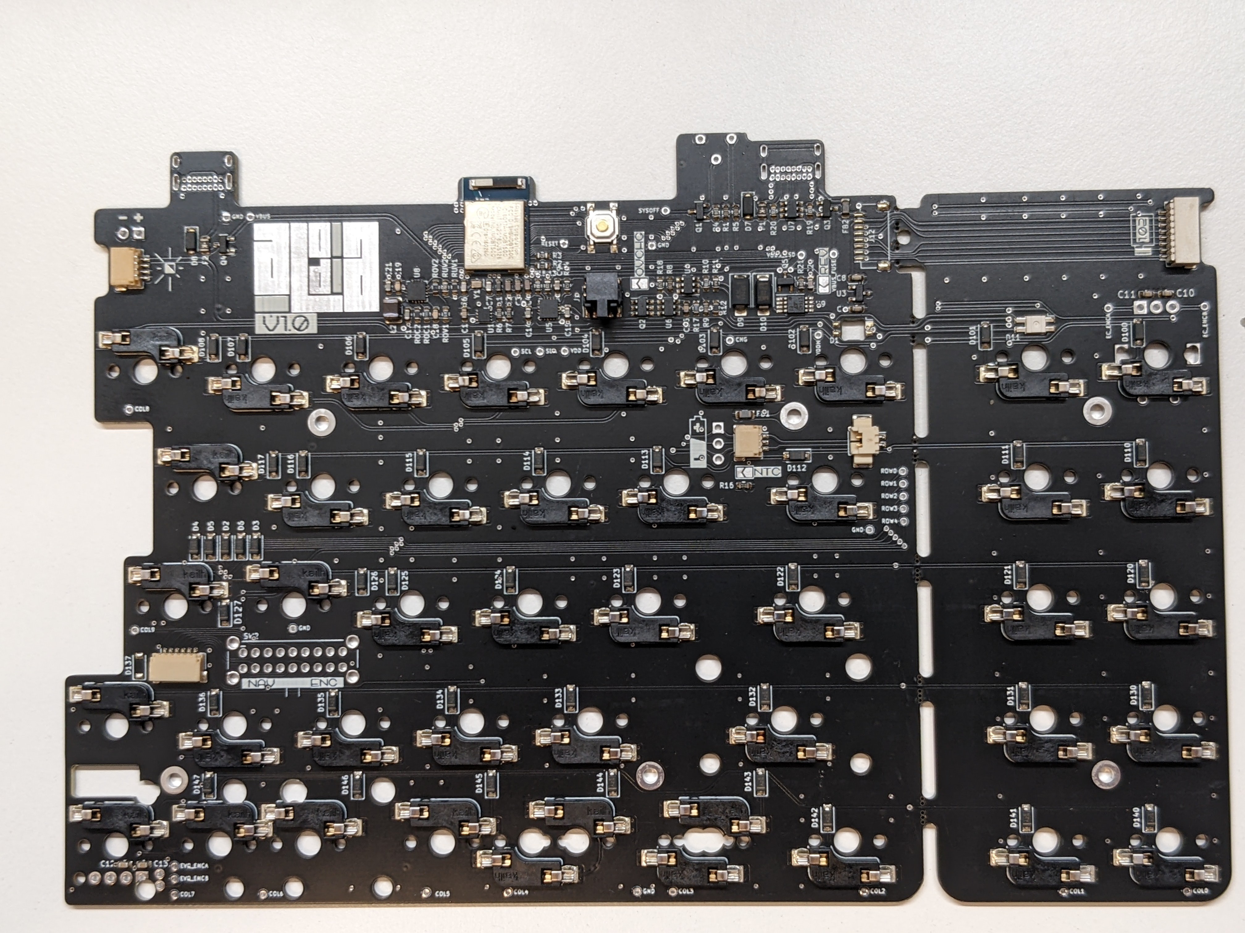
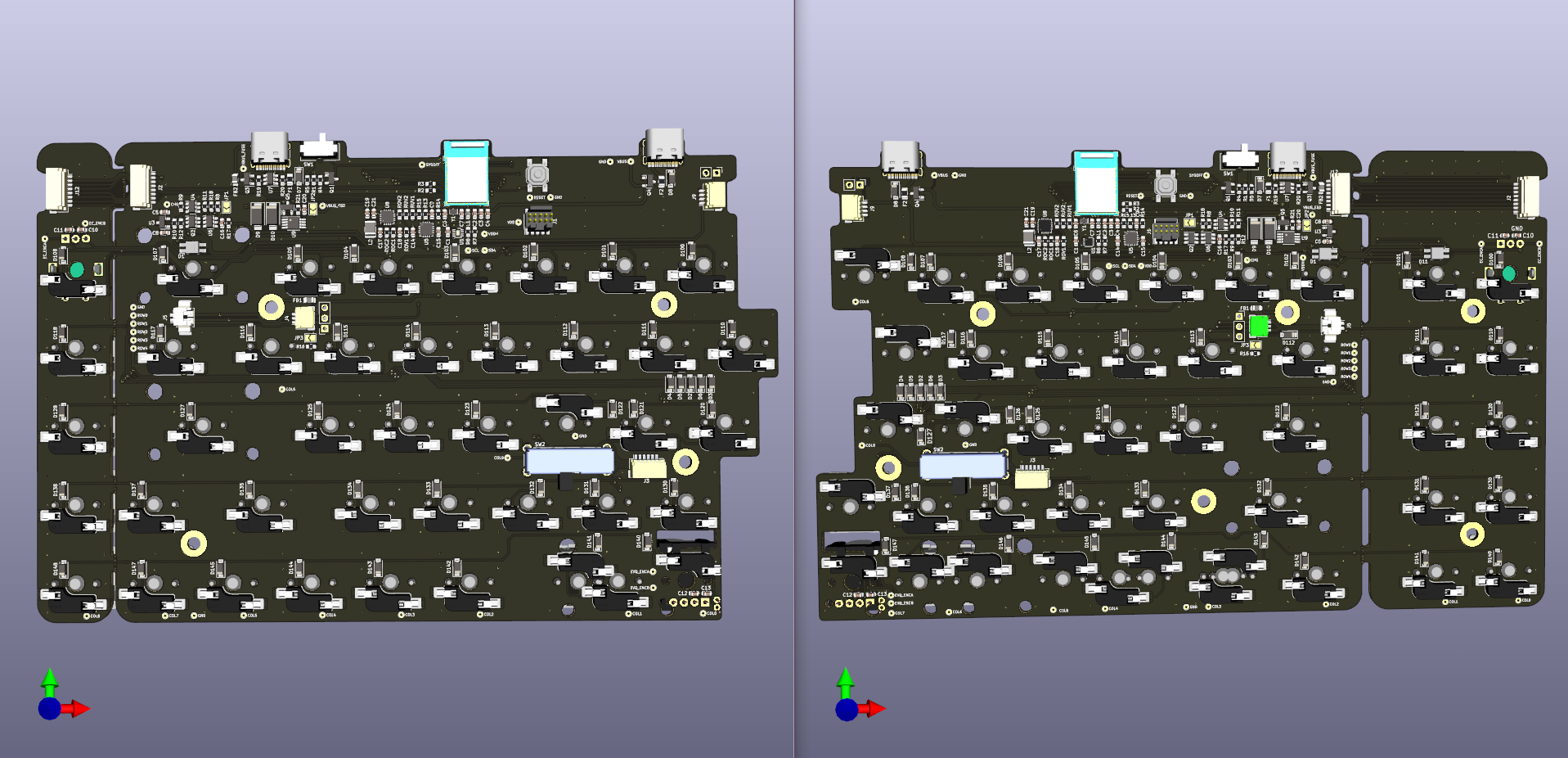
Main PCB
The MDBT50Q-1MV2 module from Raytac was used in this project. This is a very interesting module as the DCCH, VDDH, VDD and VBUS lines are all broken out. This allowed me to design the chip around its high-voltage mode, which is very useful as the internal DC-DC converter can be used. A very interesting feature of the nRF52840 is that it switches between its internal LDO and its internal DC-DC converter to maximize efficiency.
The board is also is equipped with the BQ24075 lipo-ion charger. This chip is interesting because of its interesting sets of features:
- a selectable 100mA or 500mA charging current, which is ideal for charging with USB port
- SYSOFF input, which enables the user to turn off the keyboard with an SPDT switch. This has as an advantage that when turned off, only the battery is disconnected, but the user can still use the keyboard via USB. The disadvantage is the increased power consumption, as the chip has internal pullups on the SYSOFF input.
- Thermal shutdown protection. By connecting a 3-wire battery (with the third wire being the thermistor), it's possible to shut down the system when the battery gets too hot. To make the PCB as versatile as possible, it can also support 2-wire batteries in which case a jumper has to be closed, which connecting a 10k resistor to the thermal shutdown input.
For battery protection, the AP9101CK6-ANTRG1 IC was chosen. Most people might go with the TP4056 + DW01 combo but the DW01 has its under-voltage lockout protection way too low (2.4V), which makes it useless for a standard 4.2V lipo. The AP9101CK6-ANTRG1 has its under and over-voltage cutouts at 3.4 V and 4.225 V respectively, which is much better.
To further protect the board, the USB-C inputs are protected against ESD events, reverse voltage/input, reverse current and over voltage. The LTC4359 ideal diode controller was used for highly robust protection. This might be slightly (or very) overkill for a keyboard, but I had some on hand so why not.
For the energy harvester chip, I chose the BQ25504 as it could harvest very low amount of luminous energy (even from indoors light) and had very low quiescent current. It also implements maximum power point tracking (MPPT) to maximize its energy harvesting capabilities.
To measure the battery voltage, the MAX17048 fuel gauge is chosen. This is a very inexpensive chip which communicates via I2C. I'vr chosen this chip instead of the classical voltage divider solution because of its high precision during charging phase. Indeed, lipo batteries tend to have non-linear charging curves, which could make determining the state of charge more difficult with a voltage divider. Another interesting characteristic of this chip is that it does not use any sensing resistor, which makes its footprint on the board very small.
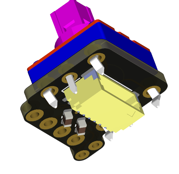
As you might have noticed, there is a large switch near the bottom half of the board. This is a 6PDT switch, which makes it possible for the user to choose between a 5-way navigation switch or an horizontal rotary encoder (EVQWGD001). They are connected to different parts of the switch matrix, and connected to the main PCB with a 6-pin JST-SH connector.
The PCB can be broken off on the sides while retaining its core functionality for a reduced layout.
![]()
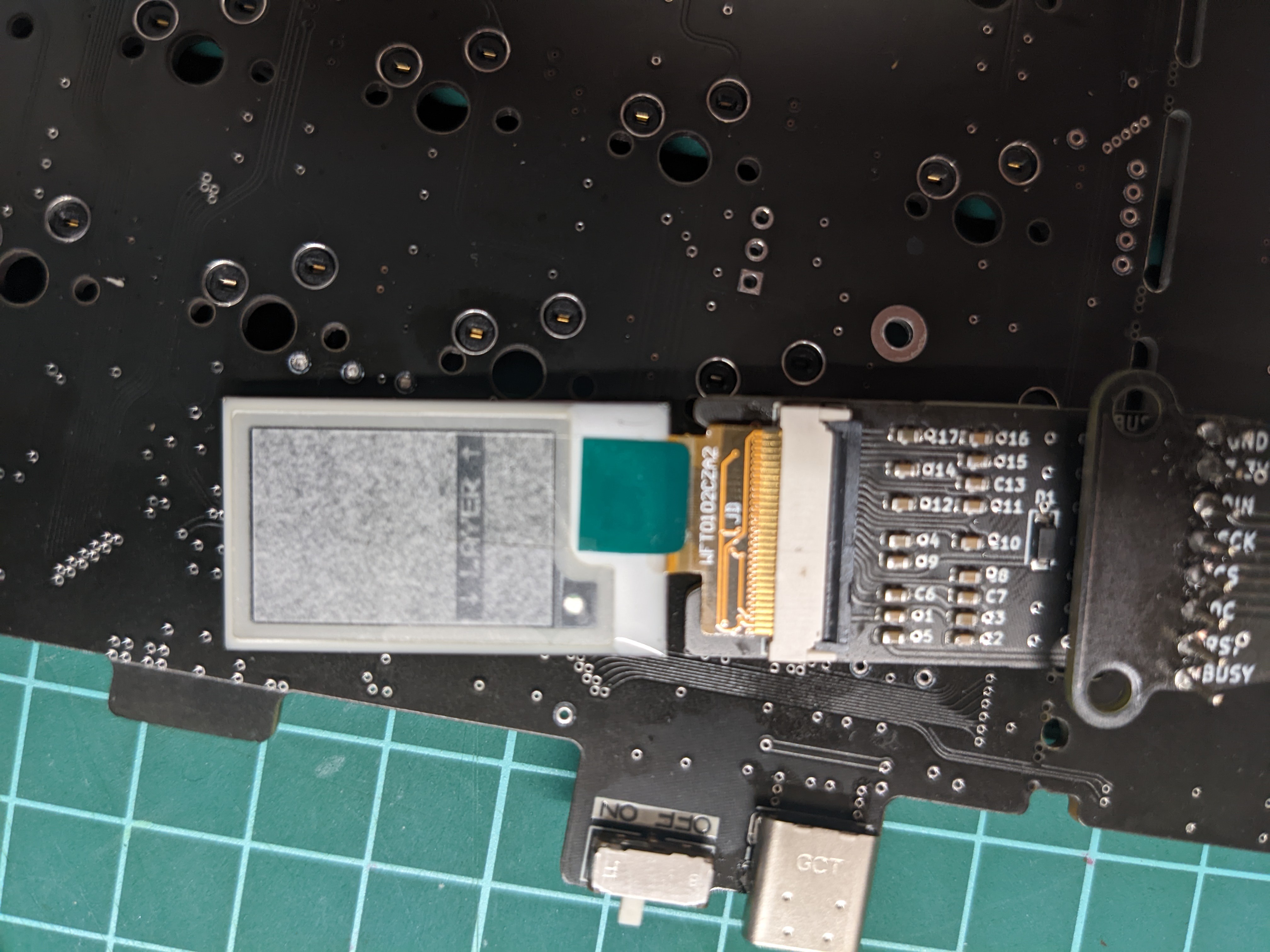
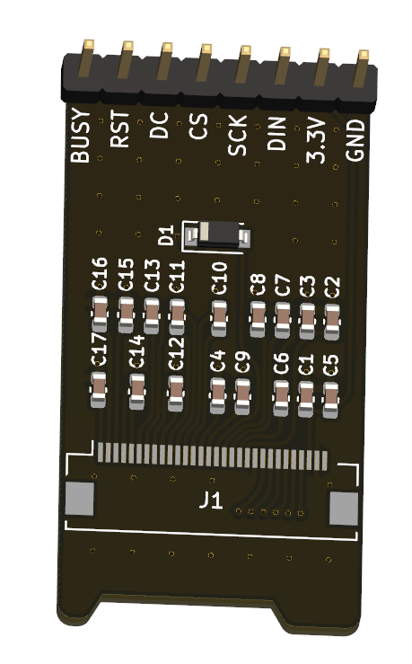
E-ink paper display breakout
It's designed for the Waveshare 1.02 inch e-paper display module. This display is quite interesting as it consumes almost no current when not refreshing, which makes it perfect for a battery-powered application.
![]()
It's connected to an adapter board as shown below. This board is crucial to provide mechanical support in the keyboard case, as I wanted the display to sit as flush as possible against the top of the case.
Solar panels
A very simple-looking PCB, which is however more complicated than it seems. The shape of this PCB is very important as the flaps serve as mechanical support against the top of the case. Indeed, the solar panels need to be flush against the top of the case to maximize efficiency, which made the design quite more complex as I wanted to have no visible screws from the top. As such, each pad here has many vias which makes it possible to solder the solar panels from the other side while pressing them against the top of the case.
![]()
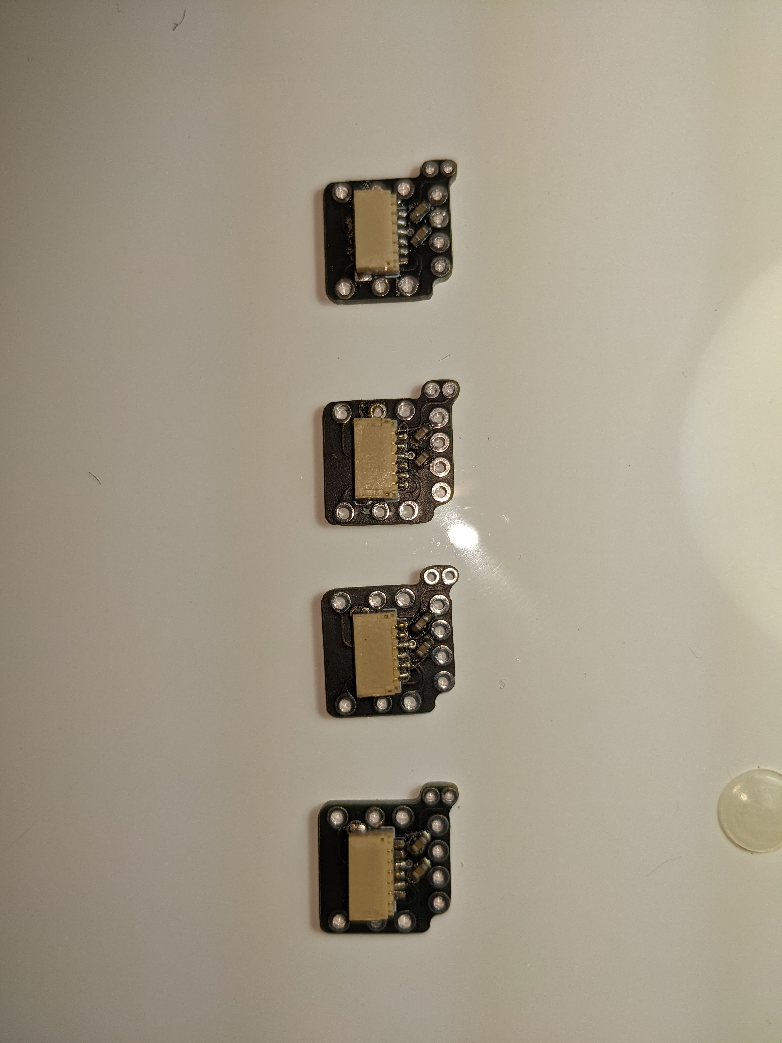
External connector
This PCB is used to connect either a 5-way navigation switch or horizontal encoder. Its shape is quite tricky, as it needed to fit inside a 1u switch (19.5 x 19.5mm) max. It exposes a 6-pin JST-SH connector which can be connected to the main board.
Aloidia: wireless split solar powered keyboard
Aloidia is a staggered, split, fully wireless solar-powered mechanical keyboard with extremely long battery life.