 zpekic
Context
Given that this CPU implementation is an almost canonical example of microcoded design as envisioned by AMD - and a showcase of their Am29XX and Am25XX ICs - it is very helpful to go over at least chapters I and II of the "Bit-slice microprocessor design" book for better understanding. After that, the application note provides a great explanation of this specific CPU implementation. All source files to implement the CPU are under this folder.
General notes
In this CPU re-creation I attempted to follow the original application note as closely as possible. The description there is very detailed but also sufficiently clear to allow not just the understanding of this implementation, but how it can be adapted to other similar processors. The schema of the CPU is in figures 3-5 in the application note, and the VHDL top-level file is organized to follow those figures, and IC names/id so that the code can easily be mapped to schema and vice versa.
VHDL has the ability to describe circuits in both structural and behavioral ways, and in any source files these can be freely mixed. In this case, top-level is mostly structural (building blocks), for example:
-- data bus register (FLAGS)
-- 7 6 5 4  3 2 1 0 --------
-- S Z 0 AC 0 P 1 C --------
        u102: Am2918 port map (     clk => CLK,
                    nOE => db(3),
                    d(3) => '1',
                    d(2) => '0',
                    d(1) => '0',
                    d(0) => u92_pin7,
                    o(3) => open,
                    o(2) => open,
                    o(1) => open,
                    o(0) => flag_cy,
                    y(3) => DBUS(1),
                    y(2) => DBUS(3),
                    y(1) => DBUS(5),
                    y(0) => DBUS(0)
                );

      u101: Am2918 port map (     clk => CLK,
                    nOE => db(3),
                    d(3) => u91_pin4,
                    d(2) => u91_pin7,
                    d(1) => u91_pin9,
                    d(0) => u91_pin12,
                    o(3) => flag_z,
                    o(2) => flag_p,
                    o(1) => flag_s,
                    o(0) => flag_ac,
                    y(3) => DBUS(6),
                    y(2) => DBUS(2),
                    y(1) => DBUS(7),
                    y(0) => DBUS(4)
                );
While the implementation of individual components in mostly behavioral (description of functionality):
entity Am2918 is
    Port ( clk : in STD_LOGIC;
           nOE : in STD_LOGIC;
           d : in STD_LOGIC_VECTOR (3 downto 0);
           o : buffer STD_LOGIC_VECTOR (3 downto 0);
           y : out STD_LOGIC_VECTOR (3 downto 0));
end Am2918;

architecture Behavioral of Am2918 is

begin

y <= o when (nOE = '0') else "ZZZZ";

load_q: process(clk, d)
begin
    if (rising_edge(clk)) then
        o <= d;
    end if;
end process;

end Behavioral;
Components
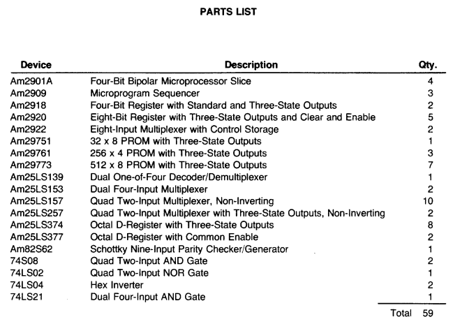
The parts list in the original design (59 ICs) closely matches the component list from the FPGA project:
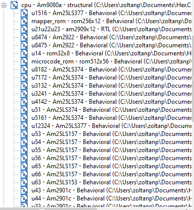
However, there are some differences for sake of simplification:
- Simple logical gates (74LSXX) are described using intrinsic VHDL logical functions, in a structural way
- 3 units of Am2909 4-bit microprogram sequencer are merged into a single fictitious Am2909-12 component to save on interconnections. This is possible as no signals between them are used. In case of Am2901 this is not possible as intermediate carry (H flag) is needed for DAA instruction
- Microcode (Am29773) and instruction mapper (Am29761) ROMs are defined as single monolith 512*56 and 256*12 ROM, initialized using memory description text files - this is described in separate project log
- The sequencer PROM (Am29751) contents is simply defined inline, not loaded from file (and is "real" size of 16*5 bits, not 32*8)
Discussions
Become a Hackaday.io Member
Create an account to leave a comment. Already have an account? Log In.