SELLING KITS
Now, there is a KIT available, to build your own Isetta !
You can order your kit at the new Envionic website ! (No HTTPS yet)
The first kit was successfully built by Vadim.
(If you want a complete Isetta, without soldering it yourself, contact me. If there is enough interest, I want to supply fully built Isetta computers, expected for around 200 euros.)
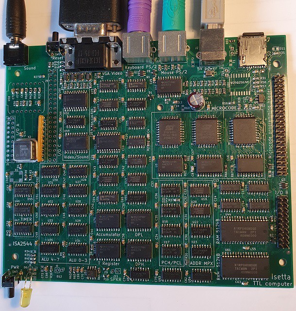
HOW DOES IT LOOK

SPECIFICATIONS
CPU:
- Runs Z80 and 6502 code
- Speed 12.5 MHz (80 nS cycle time)
- Memory 1024 kByte RAM (with bankswitching)
- programmable/upgradeable microcode (3 flash chips)
- 42 integrated TTL circuits. No microprocessor or FPGA.
I/O:
- video VGA 320 x 200 (64 colors), or 640 x 400 (16 colors)
- keyboard and mouse (both PS/2)
- sound generator (AY-3-8910 compatible)
- real time clock
- microcoded video processor, sound processor, I/O processor
- 9 integrated TTL circuits for the I/O
Storage:
- micro-SD card (removeable)
Connectivity:
- WiFi on-board (future)
- Bluetooth BLE (future)
- LoRaWan (future)
Applications:
- SymbOS operating system
- Runs CP/M (as SymbOS application)
- Runs ZX Spectrum games
- Runs several BASICs (Apple I, Altair, TRS80)
Other:
- pcb 152 x 127.5 (6 x 5 inch), 4 layers.
- powered by 5V USB
Principles for the design:
- No microprocessor, microcontroller, SOC, FPGA, CPLD, GAL, PAL or 74181
- All components have good availability at the big distributors
- Low number of components
- No fine-pitch devices that are difficult to solder (resistors, capacitors are all 0805 types)
DISCUSSION
For questions or tips/remarks you can use the discussion section at the end of the main page. Or you can send a PM, join the discussion at the RetrocomputingForum / Isetta, or use the email address at the contact page of envionic.com.
BTW, where do you come from ?
IDEA
The idea for this design was born at the end of januari (2023).
The heart of a computer is the CPU. In most computers, the CPU is a single integrated circuit (a Microprocessor). But it is also possible to build your own CPU from parts that perform simple functions. I wanted to build the CPU from parts of the TTL family. That are integrated circuits, that can perform elementary logic functions. They were first used in the 60's of the previous age. I use a modern version of these circuits, that use less power.
There are many homebuilt CPU's, and most of them have their own, unique instruction set. But when such a computer is built, you must make all software yourself ! It would be nice if existing software could run on the homebuilt CPU.
Therefore, I decided that for this project the CPU would use an existing instruction set.
So which instruction set to use ? The CPU inside your laptop or cellphone is much, much too complex to build. But it is possible to use an older CPU from the time when microprocessors just became available. There were two processors that can be regarded as the Beetle and the Deux Cheveaux of the beginning of the homecomputer age.
These processors are the MOS Technology 6502 and the Zilog Z80.

The 6502 is famous because it was the heart of the Apple 1, the Apple ] [, the Commodore 64, the Nintendo NES and many others. The Z80 is well known because it was used in the TRS-80, the ZX Spectrum and the MSX computers, and it was widely used to run the CP/M Operating system, see also this Z80 introduction video.
So now, I had to decide whether to use the instruction set of the 6502 or that of the Z80. But then I thought... why not build a CPU that can do both ?
I did spend a few months searching for a good design that would give good performance while not using too many parts. I think the basic design was stable at the end of march 2023. I then started with the details of the design, all described in the project logs at the end of this page.
SYMBOS OPERATING SYSTEM
Isetta can run the SymbOS operating system.
On april 3rd, 2025 it ran the first SymbOS applications. SymbOS is a pre-emptive, multitasking operating system with graphical user interface, comparable to Windows 95. On Isetta it still has several small bugs, but these are solvable [edit oct 2025: very few bugs left]. SymbOs stores its applications and data on Isetta's micro-SD card. Many applications take less than a few seconds to load.
SymbOS (Wikipedia) is available (for free) for seven different Z80-based platforms. There are more than 70 applications, also free, and it even has a spreadsheet ! It uses bankswitching to address more than 64kB. It can run several applications at the same time. For making your own programs, there is a development system similar to visual-basic (called Quigs), a C compiler, and you can program in Z80 assembler. It supports several languages (English, Spanish, German, Dutch, Turkish, Japanese) with more languages coming, and supports PS/2 keyboard layouts for 16 languages.
SymbOS was fully programmed in Z80 assembly language. To me, this looks like the most complex Z80 program ever made ! You can try SymbOS online on an MSX computer simulator.
Many thanks to Prodatron, the developer of SymbOS. Porting SymbOS to Isetta was only possible with his dedicated assistance.
CAN IT DO MORE ?
At the moment (aug 2024) it can:
- Run ZX Spectrum games, see Two Spectrum games running
- Run Steve Wozniak's Apple 1 BASIC
- Run Altair 8080 BASIC
Several more applications are planned.
ISETTA SYSTEM DIAGRAM

COMPUTER I/O LAYOUT

On the previous (first) PCB version, there was no mouse input.
CPU TECHNICAL DESCRIPTION
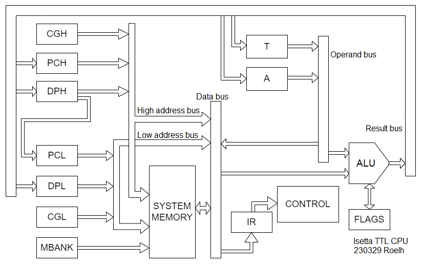
Here comes the system diagram of the CPU. Most arrows and buses represent 8 wires, that means that the information flows through the processor in units of 8 bits (a Byte).

I might as well start with explaining some of the parts.
- PCH/PCL (Program counter high byte and low byte)
- A (Accumulator register)
- T (Temporary register)
- DPH/DPL (Data pointer high byte and low byte)
- IR (Instruction register)
- CGH Constant generator, generates only 0 (mainly for zpage addressing)
- CGL Constant generator for small integer values
- MBANK Bank selection system
- ALU Arithmetic logic unit (Wikipedia) (described in project log 2)
You will miss the 6502 registers S (stack pointer) and the index registers X and Y. And you will miss the long list of registers that are inside a Z80 CPU. All those registers are in memory. A special memory section (outside the normal 64K range) is used for the registers (addressed by CGH/CGL).
In the first project log you find how the information flows through the processor.
The control section will use microcode to run the whole show. The microcode has 16 pages, 1 page is needed for the 6502 and 5 will be needed for the Z80, and the software can switch between 6502 and Z80. The microcode has room for a few more instruction sets. In this log the 24-bit microcode instructions are described with all details.
[ edit: the design was simplified, see project log 13 ]
CPU LAYOUT

On the previous (first) PCB version, there was no bankswitching.
PERFORMANCE
The clock frequency of the processor will be at least 6.25 MHz (1/4 of the VGA video clock frequency).
In october 2023 I did some timing calculations and found that the processor could, after a few changes and using faster parts, reach 12.5 MHz clock speed. The first prototype will tell if my calculations are correct. [edit: Yes, it worked ! ]
The video output is directly generated by the CPU, so this will use a lot of CPU power. (As an option, a stand-alone video system could be used).
For each instruction, generally the number of clock cycles differs from that on a real 6502 or Z80. Precise specifications of the number of clock cycles for each instruction can be found in the file section.
6502
For the 6502, the cpu will run many instructions in about the same number of clock cycles as a real 6502, but some instructions will take more cycles. But since the clock frequency is higher, it will run programs faster than the original 2 MHz 6502.
There is a very nice Overview of 6502 instructions by Michael Steil.
There will be some restrictions, decimal mode might not be implemented.
Z80
Many Z80 instructions take much less cycles on Isetta than on the real Z80. These are mostly quite simple instructions, but they are used a lot. The improvement is mainly caused by the fact that Isetta can access memory in a single cycle, where the Z80 needs three cycles for most memory accesses.
Note the improvement for LDIR, done by unrolling the loop in microcode.

But not all instructions show such an improvement. Most instructions that involve shifts, stack or 8-bit arithmetic and logic take about the same amount of cycles as the Zilog. And there are a few that are slower than on the Z80: EX AF,AF' and EX DE,HL take almost 3 times as many cycles (but EXX takes 4 cycles, same as on Z80).
So, programs will run faster than on an original 4 MHz Z80.
Information about the Z80 instructions can be found in the Z80 CPU User Manual and on the Z80info page. The officially undocumented operations on the halves of IX and IY are also supported.
The parity flag, and decimal adjust are not supported.
PROJECT LOGS
3. Requirements for the control section
7. Javascript emulator runs Apple 1 BASIC
8. Another interesting BASIC to test the 8080 instructions
9. Update
11. Video system
12. Colors
13. Less parts and higher speed
14. Re-started PCB design in SMD
16. PCB finished, Logisim simulator and programmer
18. The real hardware runs Apple 1 BASIC !
19. Moving Z80 binaries to Isetta and run them
20. File system and command shell
21. Who is afraid of Red, Green and Blue ?
22. Trying to get a ZX spectrum game running
23. Two Spectrum games working
24. Hardware changes and bankswitching
25. On the cover of the hack a day
27. Fixing the LDIR instruction
28. Changed bankswitching system
29. Second PCB version ordered
31. Announcing kits on the last day of 2024 !
32. Programming manual, microcode and Blitter
33. Come and see Isetta running SymbOS
34. Do-It-Yourself KIT available
38. One Megabyte !