In this log I talk about the 24 control signals that come from the microcode. The names of all signals that come from the microcode register will start with CTL.
[ EDIT March 2024. Since the writing of this log, several details have changed, so this log is no longer fully accurate ]
The microcode will be organized in 3 bytes, the upper, middle, and lower control byte. The upper microcode has the longest description.
MICROCODE UPPER CONTROL BYTE
The first diagram shows the signals that select a condition and handles flags:
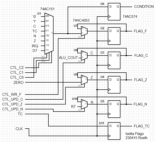
Flag update
Some instructions update flags, others don't. The signals CTL_UPD_C, CTL_UPD_Z and CTL_UPD_N indicate if the flags C, Z or N must be updated with a new value coming from the ALU_COUT, the ZERO detector at the output of the ALU, or bit 7 of the ALU output (R7, Result-bus bit7). If a flag is not updated, it will keep the same value.
There is no provision to read or write the flag bits as a full byte, like that is normally used in many 6502 designs. The microcode will have to read or write the flags one-by-one in order to push or pull the flags (or do EX AF,AF' for Z80).
Condition select
The signals CTL_C0, CTL_C1 and CTL_C2 select one of eight conditions. It is used for two different things:
- As a selector of the CONDITION carry-in signal of the ALU (adder or shift-right)
- As a selector for the FLAG_F for conditional execution. This second function is activated when CTL_WR_F is active (high). If CTL_WR_F is low, FLAG_F keeps the same value.
Early condition evaluation
There is one more important thing to say about the condition selection. Suppose that we want tot test for a condition, and execute a conditional micro-instruction based on that, this would be 3 micro-instructions (3 cycles):
- Select the relevant condition, like C, Z or N, (putting this condition in FLAG_F)
- Fetch the next micro-instruction based on the FLAG_F value
- Execute the micro-instruction that was selected with FLAG_F
Number 1 and 3 are really needed, but in number 2 we are just waiting for the next micro-instruction coming out of the pipeline, and if we can not do something useful in that cycle, it is a 'lost cycle'. But we can do something about that. By connecting the signals CTL_C0, CTL_C1, CTL_C2 and CTL_WR_F not to the microcode register, but directly to the microcode ROM output, we can evaluate the condition one cycle earlier (at the end of the fetch phase). We now get the following two-cycle sequence:
- Select the condition. The selection has actually been done in the previous cycle, so in this cycle the new micro-instruction, based on the FLAG_F value, will be fetched.
- Execute the micro-instruction that was selected with FLAG_F
So we just gained one cycle for micro-instructions that use conditional execution.
ALU CONTROL
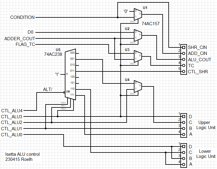
The ALU control section must provide the control signals for the ALU. In the ALU log it is shown that the following control signals are needed:
- 4 bits DCBA controls for the upper logic unit
- 4 bits DCBA controls for the lower logic unit
- 2 bits Carry-input signals for added (ADD_CIN) and right-shift (SHR_CIN)
- 1 bit selection of shift-right unit CTL_SHR
So the ALU can be controlled with 11 signals. But we don't want to spend so many of the available micro-instruction bits for these. Fortunately, it is not difficult to bring this number of signals down to a reasonable amount.
Generating the DCBA control signals
The DCBA controls for the upper logic unit have bit A being '1' only in the case of a DEC instruction (and for complementing a value, but we don't use that). So bit A can be removed from the control wires and be regarded as a special case.
The DCBA controls for the lower logic unit only use the patterns 0000, 1010 and 0101. Of these, the 0101 is only used in a single case (SUB, Subtract), so if we handle that as a special case we only need a single control signal CTL_ALU0 for choosing between 0000 and 1010.
To handle the special cases, we have a decoder (U5) that decodes the CTL_ALU1, CTL_ALU2 and CTL_ALU3 lines into 8 separate cases. The output of the decoder is activated (high) when the ALT/ signal is low. It handles the DEC and SUB cases and will also control the right-shift (CTL_SHR) as a special case.
Group 0 and group 1
The ALU operations are divided in two groups, selected by CTL_ALU3:
- Group0, when CTL_ALU3 = 0
- Group1, when CTL_ALU3 = 1
Group1 is the easiest to understand, this encompasses all arithmetic instructions (although also some logical instructions are in this group). The multiplexers at the right side of the drawing will do the following:
- U1 will connect the CONDITION to the carry-input of the adder
- U2 will connect the carry-output of the adder to the ALU carry result
- U3 will update TC (temporary carry) with the value of the carry-output of the adder
- U4 will connect CTL_ALU2 to bit C of the upper logic unit, providing all 1xx0 functions
Group0 encompasses instructions where the adder is only used as pass-through, for some logic functions, for shift-right and for loading (moving) a value. This is also the group to use for writing a new value to FLAG_F. A single micro-instruction can write to FLAG_F and load a new value (at the same time). Multiplexer functions for group0 are:
- U1 will disconnect the carry-input of the adder from the CONDITION. If the condition is used to write FLAG_F or to provide carry-input to shift-right, the adder should pass-through any value unchanged, and having a signal on its carry-input would spoil the pass-through.
- U2 will connect databus bit D0 to the ALU carry result, for the case that a shift-right is done, where D0 is shifted out of the byte and can be put in the carry C.
- U3 will load TC with its own value, so it will not change. So when a byte was added to a low byte and this might have set TC, we can do some data move instructions afterwards, and still have the TC available to use it when adding something to the high byte.
- U4 will connect bit C of the upper logic unit to output 001 of the ALT decoder (U5). This makes the value 0000 appear twice in the range of codes. This is a useful code because it enables the LD (pass) function of the ALU. Having two LD functions means that we can combine it with two different special ALT cases (to be discussed later). When the output 001 of the U5 decoder is selected, we can use the ALT/ signal to switch between 0010 (RES function) and 0110 (EOR/XOR function). The RES function is a bitwise logical function, that resets a bit coming from the databus when a bit on the operand bus is set (useful for Z80).
Summary of upper control byte
The upper control byte has the five ALU controls in bits0-4 and the three condition selects in bits 5-7. The following diagram shows the ALU micro-instructions that are possible with the upper byte:
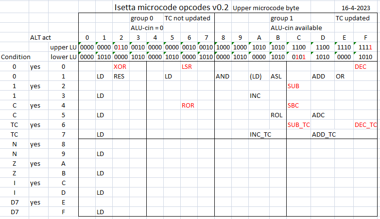
- The functions that need an active ALT are shown in red, and the control bits in the upper and lower logic units are also in red if they are modified by this ALT function.
- You can see in column 1 that the LD function can be combined with every condition (to be put in FLAG_F)
- In column A there is also a (LD) function but this does not have the benefits of the LD in group 0.
- All empty positions will also perform functions but these functions will in many cases not be useful.
MICROCODE MIDDLE CONTROL BYTE
This will provide the following control bits (explained below):
- bit7 CTL_SRC
- bit6 CTL_DST2
- bit5 CTL_DST1
- bit4 CTL_DST0
- bit3 CTL_WR_F (see condition select at the beginning of this log)
- bit2 CTL_REG3 (extension to reg0/reg1/reg2 in lower control byte)
- bit1 CTL_M1
- bit0 CTL_M0
Source and Destination
Most bits in this byte determine how the information flows in the CPU. A source and a destination are selected. The CTL_DST0, CTL_DST1 and CTL_DST2 determine the destination of a byte on the result bus:
- 0, Register T
- 1, DPH register
- 2, DPL register
- 3, Memory
- 4, Register A
- 5, PCH register (PCL will at the same time be loaded from DPH)
- 6, VRAM (Writes to video RAM)
- 7, Output (to be defined later)
The bit CTL_SRC determines the source for the databus. For destinations Memory and Output, the source is:
- CTL_SRC = 0, source is the lower control byte of the microcode register
- CTL_SRC = 1, source is the operand bus (with destination Memory, used for storing register A or T to memory)
For destinations other than Memory or Output, the source is:
- CTL_SRC = 0, source is a byte coming from the high or low address bus (see CTL_HI in lower control byte)
- CTL_SRC = 1, source is a byte coming from memory
Address
Almost all source and destination combinations need an address on the address bus. The address is determined by the CTL_M0 and CTL_M1 signals:
- 0, a register stored in memory, addressed by the CGL constant as low byte and a zero as high byte
- 1, a zero page address (for 6502), addressed by the DPL register, with high byte zero
- 2, the program address, addressed by PCH and PCL
- 3, a full 64k address, provided by DPH and DPL
When the program counter is used to address memory, it will also increment. But if it's only used to access its value (like for storing a return address), it is not incremented.
MICROCODE LOWER CONTROL BYTE
This will provide the following control bits (explained below):
- bit7 CTL_ACC_A (If high, A is on operand bus. If low, T is on operand bus)
- bit6 CTL_UPD_C (tells if C flag must be updated)
- bit5 CTL_UPD_Z (tells if Z flag must be updated)
- bit4 CTL_UPD_N (tells if N flag must be updated)
- bit3 CTL_HI
- bit2 CTL_REG2
- bit1 CTL_REG1
- bit0 CTL_REG0
When the source is coming from the high or low address bus, it comes from the high address bus if CTL_HI is '1', and from the low address bus if CTL_HI is '0'.
In the register addressing mode, the lower 3 bits specify 8 registers. If the CTL_HI bit is set, it specifies 8 other registers, but in this case there is an extra address bit that is provided by the Z80-exx flipflop. The result is that the upper 8 registers can be swapped for other registers by toggling this flipflop. It implements the alternative register set of the Z80.
Well, that's it. I hope I didn't forget a control bit.
The drawings in this log were made with Scheme-it.
Discussions
Become a Hackaday.io Member
Create an account to leave a comment. Already have an account? Log In.