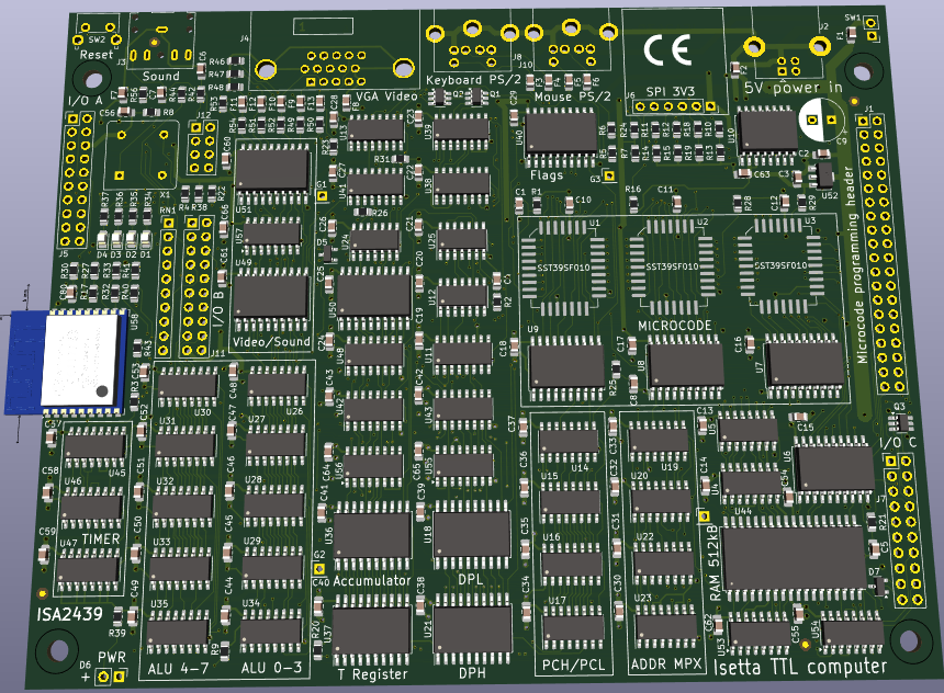
Here is an impression of the new PCB (Image generated by KiCad). It's almost finished.
And here is a small section (of four IC's) :

The TOP layer is RED, first inner layer is groundplane (not shown), second inner layer is ORANGE and the BOTTOM layer is BLUE. You can click on the picture for a better view.
Yes, all routed by hand.
Discussions
Become a Hackaday.io Member
Create an account to leave a comment. Already have an account? Log In.