 Arya
Arya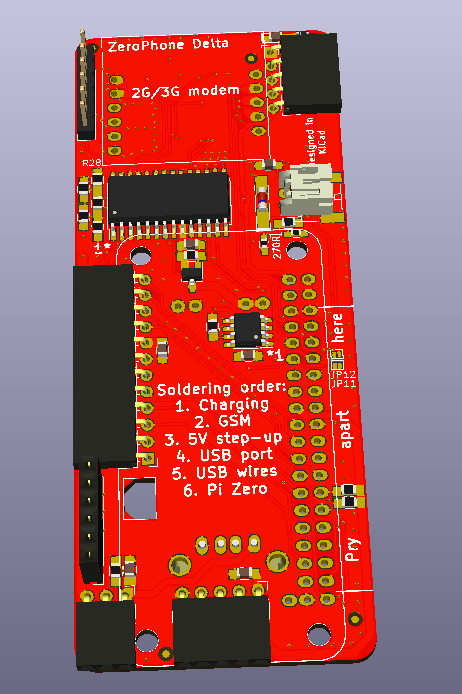
The new revision, ZeroPhone Delta, is out. I've been using a Gamma ZeroPhone for quite some time now, and it needs some bugfixes. Specifically, I:
- Fixed a mechanical weak spot where a row on the keypad would break due to lack of structural support
- Fixed tantalum capacitor footprints - now they're more solderable
- Fxed the problem where traces on the 18650 board would get exposed to the back board (and short things together) due to soldermask scraping off the back board when scratched by the back board through-hole pins
- Flipped the 3G modem upside down, making the routing significantly easier
- Reorganized the SPI (side) expansion header footprint, changing it to use 12-pin headers (easier to source)
- Reorganized the I2C expansion header to be compatible with the Raspberry Pi I2C pinout, allowing to connect existing I2C RPi expansion boards to ZeroPhone
- Reorganized the IR (top) expansion header - now it's safe to plug expansion boards in reverse
- Audio buffer, vibromotor and keypad backlight circuits are now powered from VSYS
- Flipped the DC-DC power FET so it's no longer necessary to solder it flipped
- Flipped the charger board - now it's easier to solder it, as well as swap and test
- Made the Pi Zero pads on the back board oval - making them stronger (for rework purposes)
- Changed the 4-pin GSM audio header into a 6-pin one - for easier sourcing
- Improved the microphone footprint on the front board
- Made fiducials smaller - mostly I needed more space for routing
- Improved the switchable display header - the jumper pads are now smaller, and through-hole part of it is covered by soldermask on the front of the board (to avoid displays shorting to it)
- Made the surface-mount crystal resonator pads on the front board larger, in attempt to make the resonator hand-solderable
- Added traces to the MCP23017 footprint in an attempt to make it more reworkable
Here's what I added:
- Inductors in series with GSM microphone traces - for noise filtering
- Assembly instructions/guidelines on front, back and keypad boards
- Usage instructions on the 18650 board
- Expansion header pinouts on the back board
- A comparator - detecting charger&USB undervoltage and charger board overheating
- A circuit that'd allow sensing whether the "power switch override" button is pressed while still eping the phone switched on
- An UART buffer - not connecting the GSM UART to the Pi UART until a GPIO is asserted
- UART testpoints near the charger board outline - to allow for a charging+UART board to be made
- Serial number fields on front, back and keypad boards
- An audio amplifier for the GSM speaker (unfortunately, it's a TI part - I'll be looking for a substitute)
- An I2C EEPROM to GPIO0 and GPIO1 to the back board - to make the back board work as a Pi HAT in software
- Better power filtering for the GSM modem power
- A "connect 5V DC-DC to the charger input when the DC-DC is powered off" circuit
- 3.5mm jack audio filtering to remove GSM noise
- ATMega UART header reverse polarity protection
- A fuse to the 18650 board between two batteries, to avoid problems when people insert batteries in reverse, or batteries with different levels of charge
- Finally designed the first solution to attach the GSM speaker
I also removed a lot of things that didn't prove themselves useful:
- The RTC footprint - proved to be unnecessary and incomplete, and was taking a lot of PCB real estate
- The GND-BATT- jumper - wasn't useful
- The capacitor footprint in parallel with BATT+ and BATT- - wasn't useful
- The MPU9050-compatible footprint - wasn't useful enough compared to the PCB real estate
- The second USB socket (facing the board center) - wasn't useful
- The RST and TV-OUT pad connections - weren't useful (though having a way to bring them back later would be cool, maybe add a pad for a surface-mount pin header?)
OSHPark links: 18650 board, back board, front board, keypad board and speaker adapter
Some of these points (like silkscreen additions) could be explained further, but I'll show them off once I receive the boards and make the assembly guides. This is pretty much the gist of the Delta release. There's a lot of safety, usability and reliability fixes - not so much in terms of features, but, as you know, adding things means adding bugs, and I couldn't really afford to have a lot of those in this revision. This revision is the one I'll be promoting once I get it and assemble a phone or two - I finally feel like i can put trust in a revision that I've made, and I can safely calculate the crowdfunding campaign expenses based on its BOM.
Now what? I need to do a bunch of work on software. A new SD card image is long overdue (and I really need to look into automatically building these), and I finally can work on integrating the part that deserves my attention the most - the GSM modem. I will also make a video assembling a Gamma ZeroPhone from scratch - I don't think making full-blown assembly instructions is a good idea (since even the errata takes too much time), but I'll be doing that for the Delta model.
Heads up - I've also designed a ton of expansion boards (many of them at the last couple of days before ordering). There's even a cool SPI level shifter - it shifts 3.3V to 1.8V if you insert it one way, or 3.3V to 5V if you flip it over! Hope you like them - compiling a list of them soon ;-P
Discussions
Become a Hackaday.io Member
Create an account to leave a comment. Already have an account? Log In.
Nice to see this progress...
Are you sure? yes | no
Really cool man! Thanks for the good work :)
Are you sure? yes | no