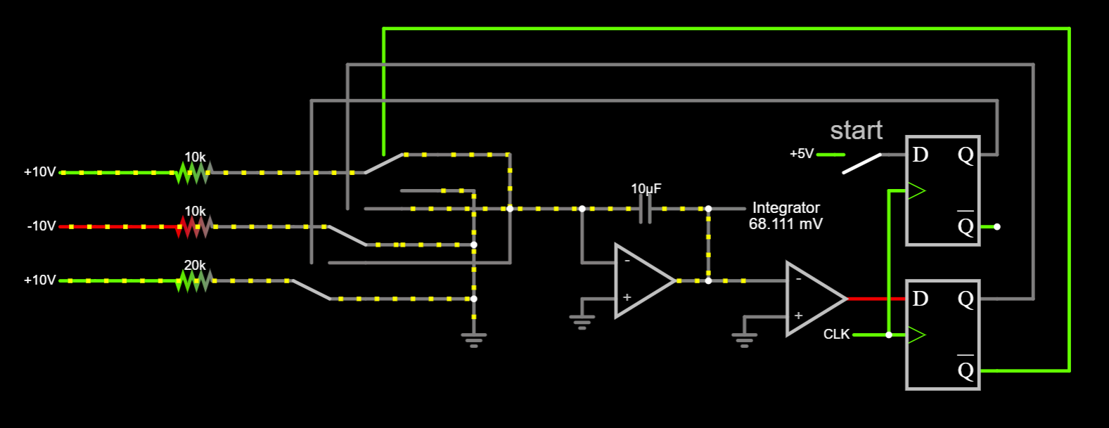
I spent a lot of time thinking about how the integrator and current switching circuit topology found in all modern multislope implementations could be improved, but all roads led me back to the same place - the circuit is almost perfect as it is:

The circuit above shows a marked difference from the simulations posted in the previous log. As per tradition, the Falstad simulation of the above circuit is here.
At the heart of the changes is the op-amp based integrator, which takes over from the plain capacitor. In this inverting configuration, the op-amp's inverting input forms a summing junction that is maintained at ground potential. This is one of the main elements that makes precision current switching possible.
Precision floating current sources are quite hard to construct. The Keithley 2002's multislope ADC features such current sources, at the cost of complexity and expensive precision resistors. Since the summing junction is held at 0V, a resistor connected to the summing junction acts like a single component V-to-I converter, with the current into the summing junction being the voltage across the resistor divided by the resistance.
The simple SPST switches have been replaced by SPDT switches. The central pole is connected to the "bottom" of the resistors, one terminal to the summing junction, and one to ground. It might seem like SPST switches would suffice, but if that were the case, the reference voltages (which are usually derived from an op-amp) would see a changing load between 0A and the reference current at several kilohertz. Precision op-amps, which are used to derive the reference voltages, usually have a low bandwidth and cannot respond quickly to load changes. This leads to reference instability and overall measurement inaccuracy. By using an SPDT switch to steer current between ground and the summing junction, a constant current is drawn from the reference voltage. This helps with accuracy and stability. All terminals of the switch are also held at a constant voltage, eliminating to a large extent a crippling parasitic effect present in almost all CMOS analog switches called charge injection.
 NNNI
NNNI
Discussions
Become a Hackaday.io Member
Create an account to leave a comment. Already have an account? Log In.