 mrpendent
Let's have a look at the schematic I had:

At least two things should jump out at anyone who knows what they are doing. There may be more, but I don't know what I'm doing, so I can only see 2 (right now).
The first one is pretty simple: the LED

I have power coming to the LED and a ground for it. So it should turn on. However, there is no connection for the I/O, so there will be no control. In a pinch I could have manually wired those, so I wasn't that upset.
Then there's this mess:
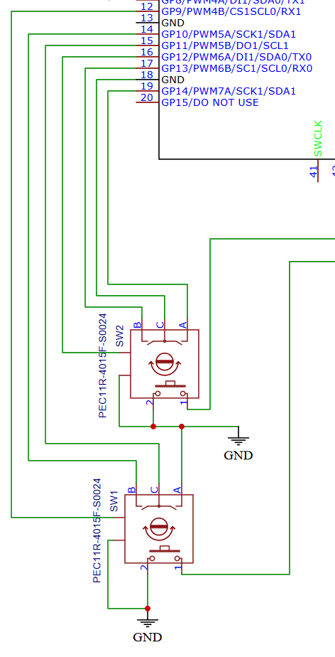
First of all, I don't know what the two extra prongs are on the encoders. When I look at my encoders, it looks like those are just metal bits to clamp it to the board (or just for decoration--what do I know?).
Even leaving that aside, we can see that the nutjob who wired this connected B and A on SW2 to GPIOs correctly. And C connected to ground.
Over on the side of SW2, though, we have a the beginnings of the weirdness. I seem to have connected two pointless prongs--one to a GPIO and one to ground. Safety first, I guess?
On SW1, we can enjoy how the A prong is wired straight into ground. Just send that signal right into oblivion. But, to make up for it, the ground prong has been wired to a GPIO!

So with this in mind, I have made a new schematic (and gerber file, of course). May I present the Grimoire Macropad v2.0 Schematic!

This makes a little more sense. then are properly connected, the LED is fully addressable, and the columns and rows are put in a place to make it easier to program the keymatrix on the Pico. So with that done, here is where the PCB is now:

The other thing that is notable here is that I have added vias in the LED pads to make it easier to connect wires, just in case. I also renumbered the switches to that they make sense--starting at SW1 in the upper left and proceeding as expected to the bottom. I moved the diodes to be under the switches after seeing that on someone else's page.
But just as I was getting ready to write this, I started hearing a tiny little voice. Just a little tiny one way in the back. A soft but wise voice saying, "You know--you probably should put LEDs under those keys..."
Dammit.
Discussions
Become a Hackaday.io Member
Create an account to leave a comment. Already have an account? Log In.