 joey castillo
Whenever starting a new microcontroller project, one of the first things to do (after, y'know, picking out a microcontroller) is assigning pins to purposes. And on this one, I've had a lot of practice: I first envisioned making a SAM L21 Feather back in 2019, long before I had the skills to design a thing like that (at least to my standards of today).
Anyway, if you clicked the link to that tweet, you'd see a photo of a table from the data sheet, along with my four-year-old notes on what I thought each pin might do. Some of those pin assignments were set in stone; PA24 and PA25, for example, are the only USB-capable pins. Same with PA30 and PA31 for SWCLK and SWDIO. But beyond that, there's a lot of flexibility in how you choose to assign pins to the things you want to do, and especially for a dev board like a Feather, we want to choose to expose pins with the most functionality possible to the end user of our board.
Pin Multiplexing Overview
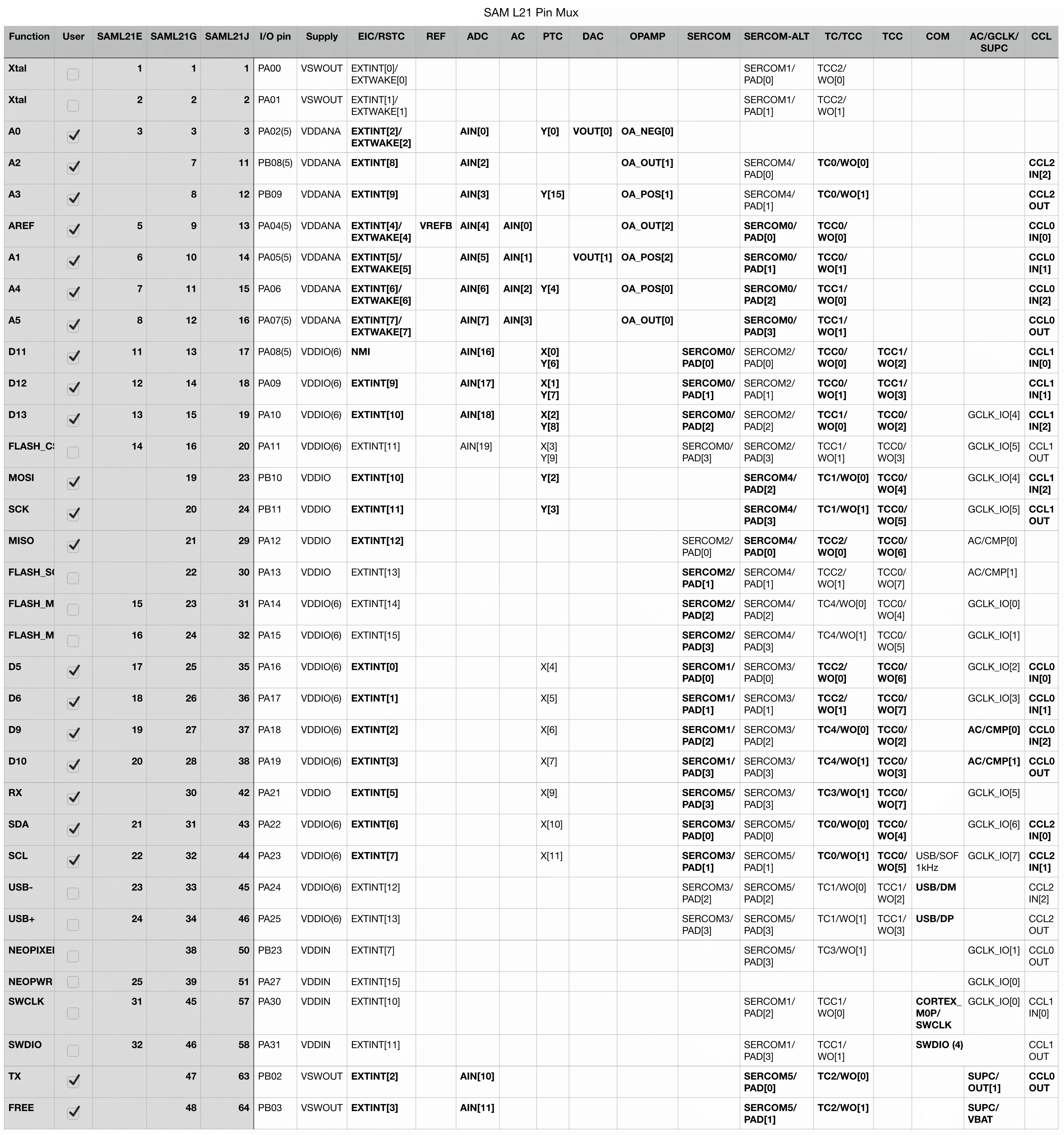
It will not shock you to learn that years later, revisiting this project with more experience and skill, I made different choices. There's a lot to unpack here, but it might be easier to walk through this if we understand roughly what we're trying to do. First off, let's look at the top line of the pin mux table in the SAM L21 data sheet:
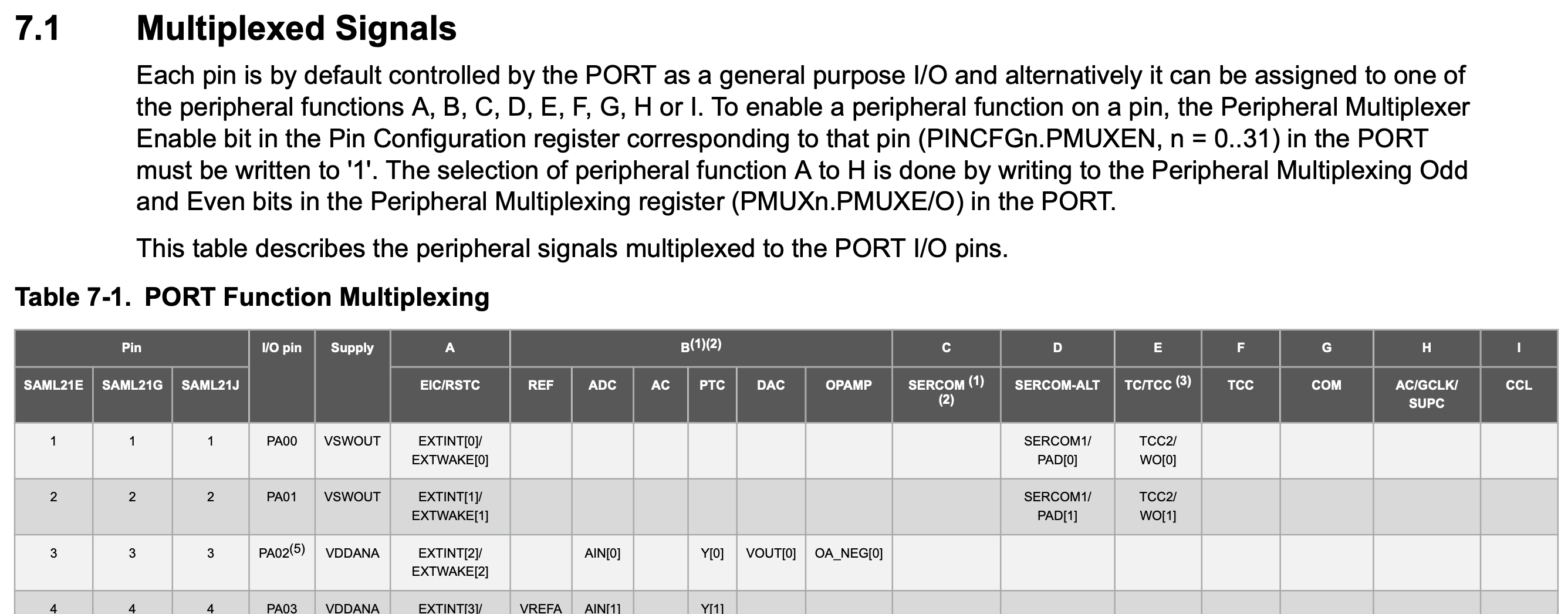
What it's telling us here is that while these pins can be general purpose IO pins, they can also be assigned to different peripheral functions that are described in that top header row. What are those peripherals? Let's walk from left to right, starting with the column named A:
- Function A connects to the External Interrupt Controller and the Reset Controller, which lets changes to pin state fire interrupts and wake the device from deep sleep.
- Function B is the analog system, which encompasses a bunch of subsystems:
- REF is the Analog Reference system, which lets analog systems make use of an external reference voltage. You might recognize this as the ARef pin on your Feather headers.
- ADC is the Analog to Digital Converter, which lets us measure analog values.
- AC is the Analog Comparator, which lets us passively compare analog values without constantly measuring them.
- PTC is the Peripheral Touch Controller, which lets us natively respond to touch inputs.
- DAC is the Digital to Analog Converter; the reverse of the ADC, it lets us output analog signals.
- And finally OPAMP is the Operational Amplifier Controller, which is kind of the name of the game here!
- Functions C and D are the Serial Communication Interfaces; these are versatile, and speak familiar protocols like SPI, I2C and UART.
- Functions E and F are the Timer Counter and Timer Counter for Control, versatile timer peripherals that can output PWM waveforms suitable for everything from beeping a buzzer to controlling a servo.
- Function G is for specialized communications; in our case, it's just the USB Interface and the Serial Wire Debug Interface.
- Function H is a hodgepodge; it has the outputs from the Analog Comparator, as well as some Generic Clock Controller pins. It also has a couple of Supply Controller pins; that system is way at the bottom of everything, literally supplying our chip with electrical power. More on that later!
- Finally, function I is the Configurable Custom Logic, which is sort of like a mini-FPGA with lookup tables and logic gates. I haven't used this much, but I want to in the future!
Goals
PHEW! That's a lot! Lest we get overwhelmed, let's take a step back and figure out what our goals are:
- I'm doing this for the Op Amp Challenge, so I want to break out all of the op amp pins, naturally.
- I need to connect the analog reference system to the Feather's ARef pin.
- I need the standard Feather features: USB, I2C, SPI and UART.
- I'd like to reserve some pins for future use: a second SPI bus for a SPI Flash chip, and a Neopixel to make it an "Express" style board.
- Beyond that, my only goal is to break out as much functionality as I can; if later I decide I want to use, say, the Analog Comparator, I want to make sure that those Analog Comparator pins are broken out.
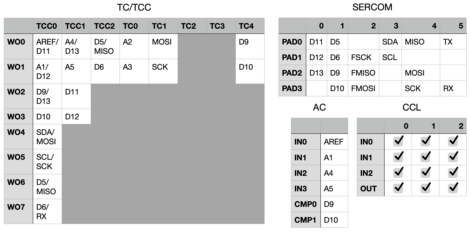
Picking Pins for One Subsystem
In fact, let's take a look at the analog system now. Here I'm highlighting just the pins related to the ADC, AC, DAC, OPAMP and REF systems:
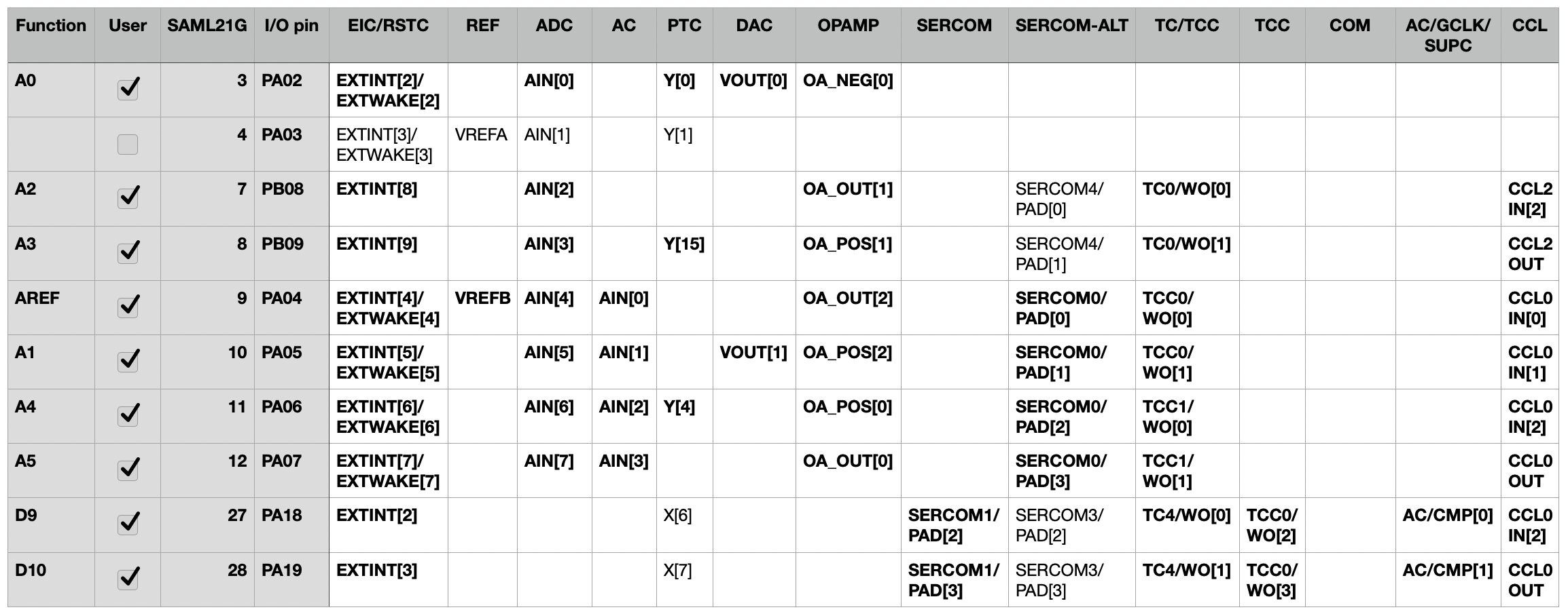
There are two pin numbers that matter here: Function is the pin I'm assigning them to on the Feather headers. I/O pin is the pin as named in the underlying firmware. And the functions on the right are the different things we can use them for. So, off to the far left, we can connect, say, I/O pin PA02 — the DAC's VOUT[0] — to pin A0 on the Feather header. It feels right that DACs should be on the first analog pins available.
For the REF system, we have two options: VREFA on PA03, and VREFB on PA04. But looking closer, PA03 doesn't do that much for us; it has a PTC channel, but other than that, it's kind of a slouch. Instead, I've claimed PA04 for the cause, because it has more alternate uses: we can use it as voltage reference B, but it also works with the analog comparator, op amp #2, a SERCOM peripheral, the TCC for PWM, or as an input to the CCL peripheral.
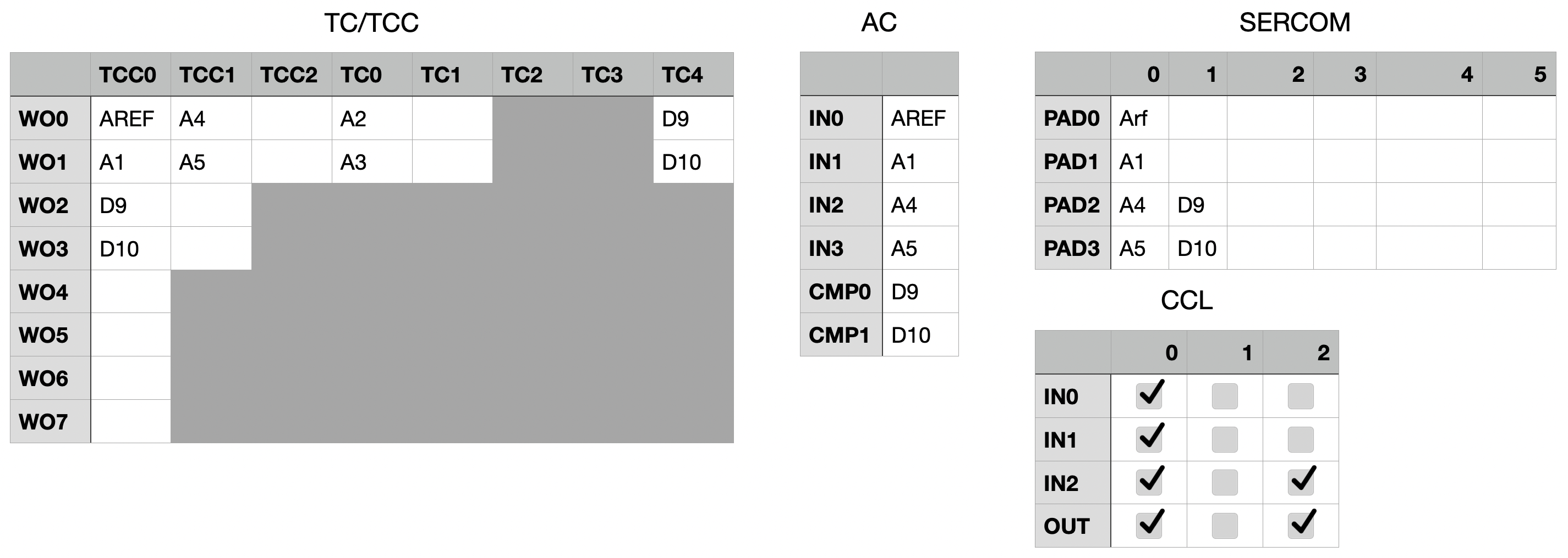
On and on we go; PA05's VOUT[1] becomes the second DAC on A1, and then A2-A4 get the remaining opamp pins. With that, we've successfully achieved goals 1 and 2 — and we're on our way to #5! Given all the alternative functions of these pins, we've already broken out two and a half SERCOMs, eight PWM outputs and six pins in the CCL!
And on and on...
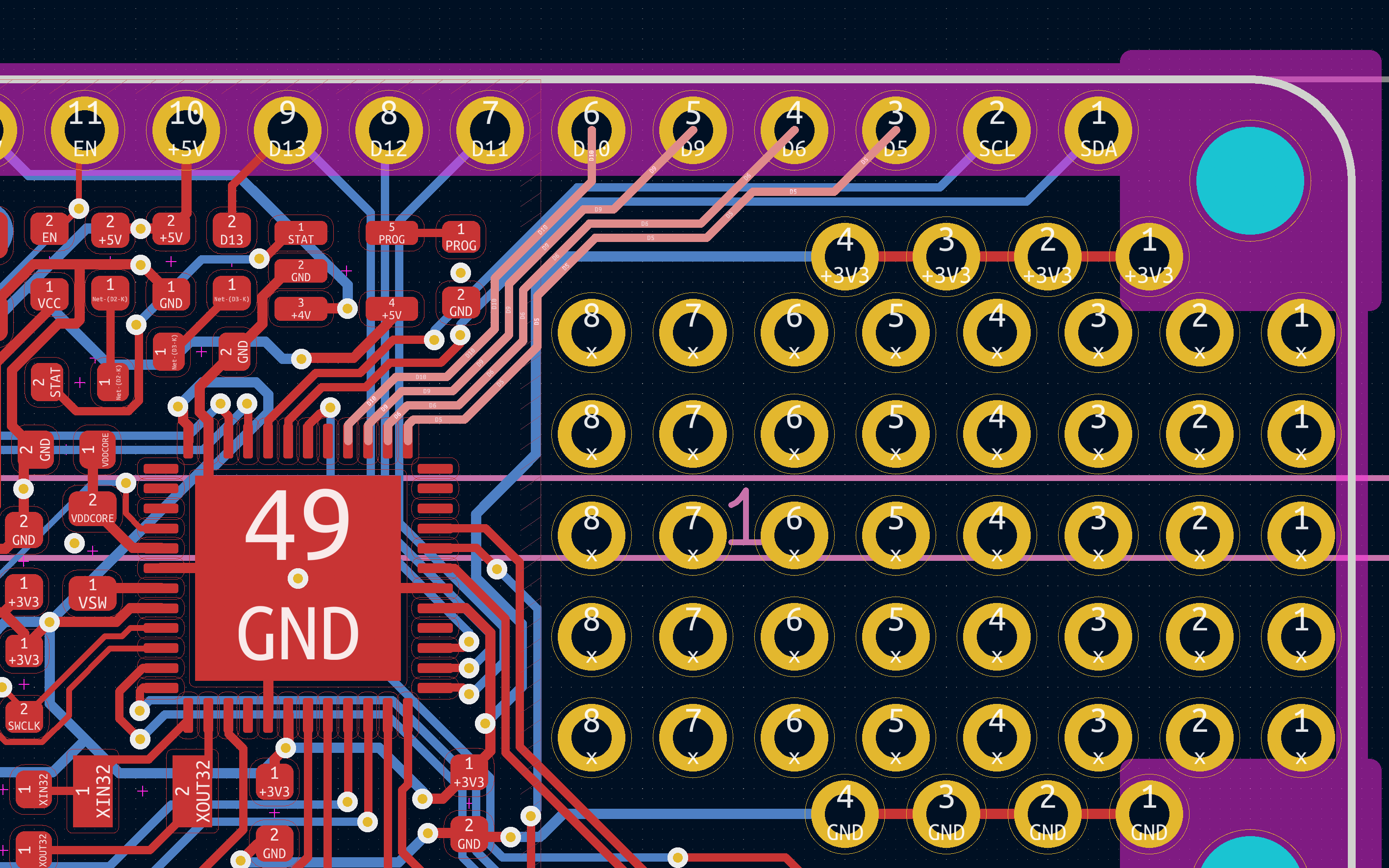
I could go on and on about this process, but let's do the rest in broad strokes: For goal #3, we need to find three free SERCOMs (two pins each for I2C and UART, and three for the SPI bus). Goal #4 is much the same: four pins for a Flash SPI bus, and two for Neopixel and Neopixel power. Chewing through the list, it sometimes feels like solving a crossword puzzle. Other times, it feels like solving a maze; in the screenshot below, once I considered routing, it felt only natural that pins 5, 6, 9 and 10 would connect to the top right of the chip; there really weren't many other options.
Final Answer
To make a long story, well, not short, but less long: here in all its glory is the pin mux for the new Feather Low Energy. The gist:
- External 32 kHz crystal for timekeeping
- All op amp pins on A0-A5 (and ARef)
- DACs on A0 and A1
- AC inputs on ARef, A1, A4 and A5
- PWM on all regular Feather pins except A0:
- All eight pins of TCC0 for NeoPXL8 goodness
- All four pins of TCC1
- Both pins of TCC2, TC0, TC1 and TC4
- SERCOMs 3, 4 and 5 dedicated to I2C, SPI and UART
- Extra SERCOMs 0 and 1 available on the top row
- SERCOM2 reserved for a Flash chip
- All CCL inputs and outputs available on pins
- Supply controller's low power output is broken out on the TX pin
- Supply controller's battery backup input is broken out on the extra "free" Feather pin at the bottom right
I think this is the most optimized possible pin selection for a SAM L21 Feather board. I think it will serve me well in the Op Amp Challenge, and I foresee it making its way in to many more projects in the future.
Discussions
Become a Hackaday.io Member
Create an account to leave a comment. Already have an account? Log In.