When starting the project, I had several requirements on my mind:
- Single supply operation, preferably in the range 9-12V.
- No trimming should be necessary to obtain reasonable accuracy.
- No "exotic" parts nor part values (especially resstors!) should be used.
- Possibly low current consumption of the circuit. (not met that well!)
- Possibly a single sided board that can be produced by a simple "Chinese" CNC mill.
The circuit I used is shown below:
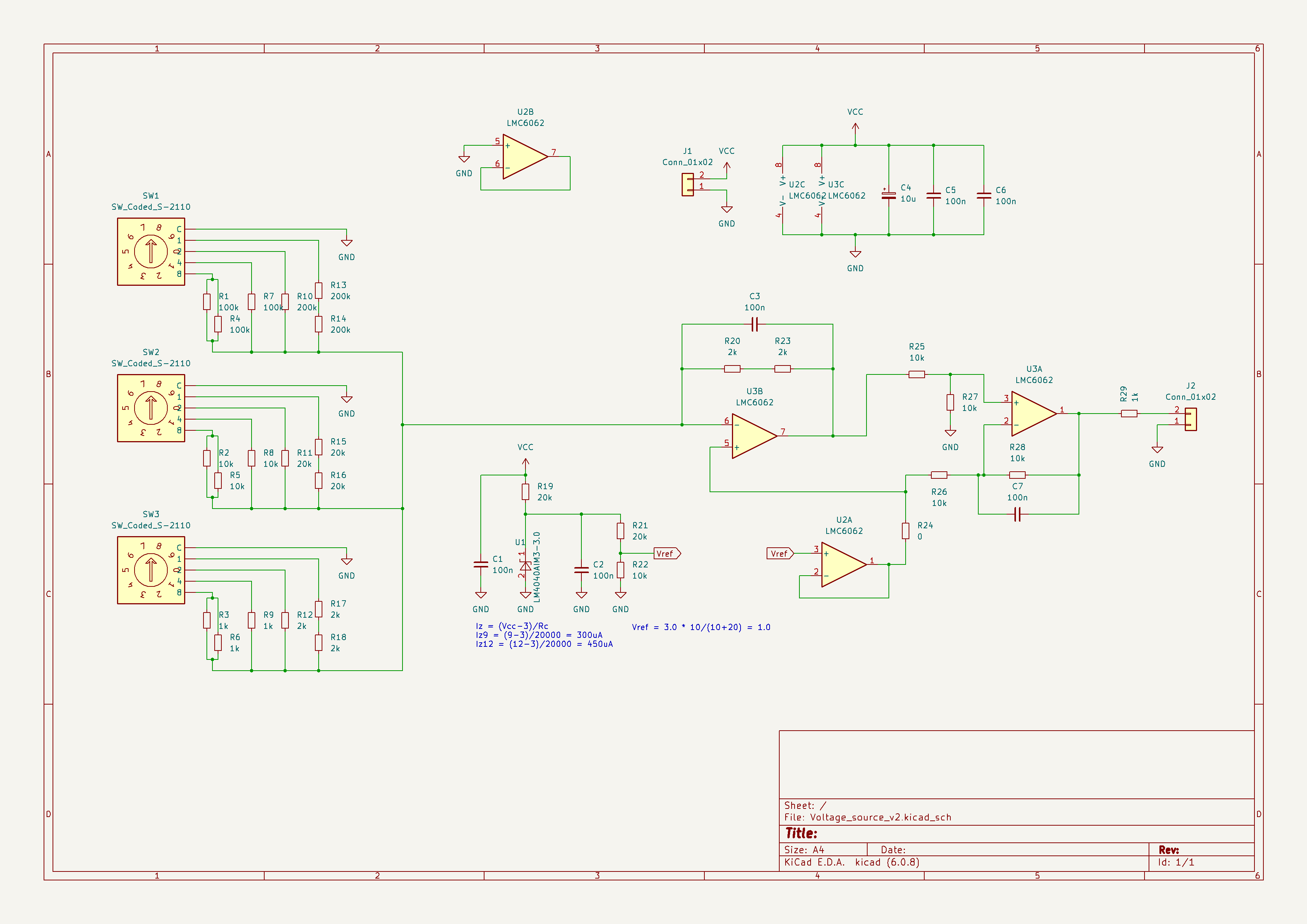
Details of the circuit
Reference voltage source
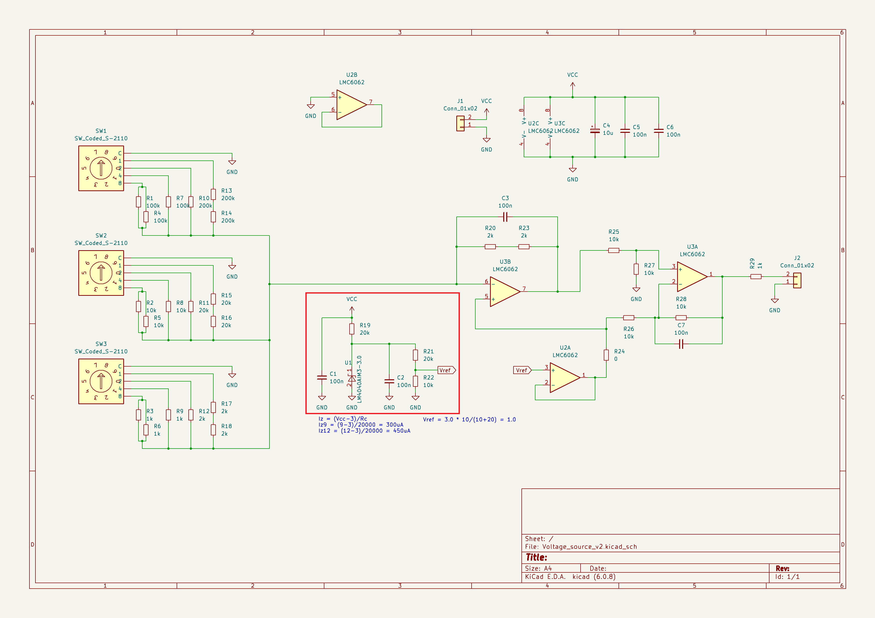
The principle of operation of the circuit starts with a stable and accurate reference voltage. I needed this to be 1V to make the simple setting of output voltage possible. In fact, any integer value of the reference voltage would do, but 1V seemed to be easy to obtain and required no "difficult" resistor values.
To produce the 1V reference voltage without using any trimmers, the LM4040A circuit is chosen. The A version may be more expensive (approximately twice the cost), but provides better accuracy. This accuracy would be degraded by further processing steps, so it is good to start with better accuracy.
LM4040 has a version that produces 3V on the output and it seems to be widely available. To produce 1V, the output voltage has to be divided in ratio 1/3, and that requires a resistor divider with values R + 2R. Luckily, values like 1k and 2k, 10k and 20k are easily available, so this was the way to go. I used precise 0.1% resistors R21 and R22 in the divider. The value of R19 does not need to be precise - a 1% or even 5% resistor should do. The value of R19 (20k) is chosen so that a sufficient current is provided for LM4040 to function properly. For the assumed supply voltage range 9 to 12V, the LM4040 current will be in the range from 300 to 450uA, that is enough to maintain the proper operation of LM4040.
Reference voltage buffer
Since the 1V reference voltage is present on the output of a voltage divider with significant output resistance (6.67k), I use a voltage buffer to provide low output resistance of the 1V reference voltage. Decreasing this resistance proved to be essential for accurate operation of the remaining part of the circuit. Using lower resistance values in the voltage divider would not help, since to get a very low output resistance, in the order of 1 Ohm or less, would require the use of prohibitively low values of resistors and increase the voltage divider current to about 300mA.
Another aspect that needs considering is the choice of the operational amplifier. It needs to have a set of properties:
- low input bias current (in order not to introduce significant errors caused by loading of the voltage divider)
- low input offset voltage (in order not to introduce significant errors to the output voltage)
- rail to rail on input and output operation (in order to be able to work with a single supply voltage and provide wide range of output voltage)
I chose LMC6062 because I can easily get them for a reasonable price. They are precision (=low offset voltage) CMOS (=low bias current) amplifiers. The specified supply voltage is from 4.5V up to 15V. Especially the second value is important - many modern opamps do not work with supply voltage above 5.5V. LMC6062 is also a rail to rail opamp, which is important in this project. They also have quite high typical open loop voltage gain, that helps to maintain consistiency between real life performance and results of simple calculations we are used to. Plus, there are two of them in a single SO8 package.
Resistor R24 is there only to help in routing the tracks on the PCB and its value is 0 Ohms.
Voltage generator
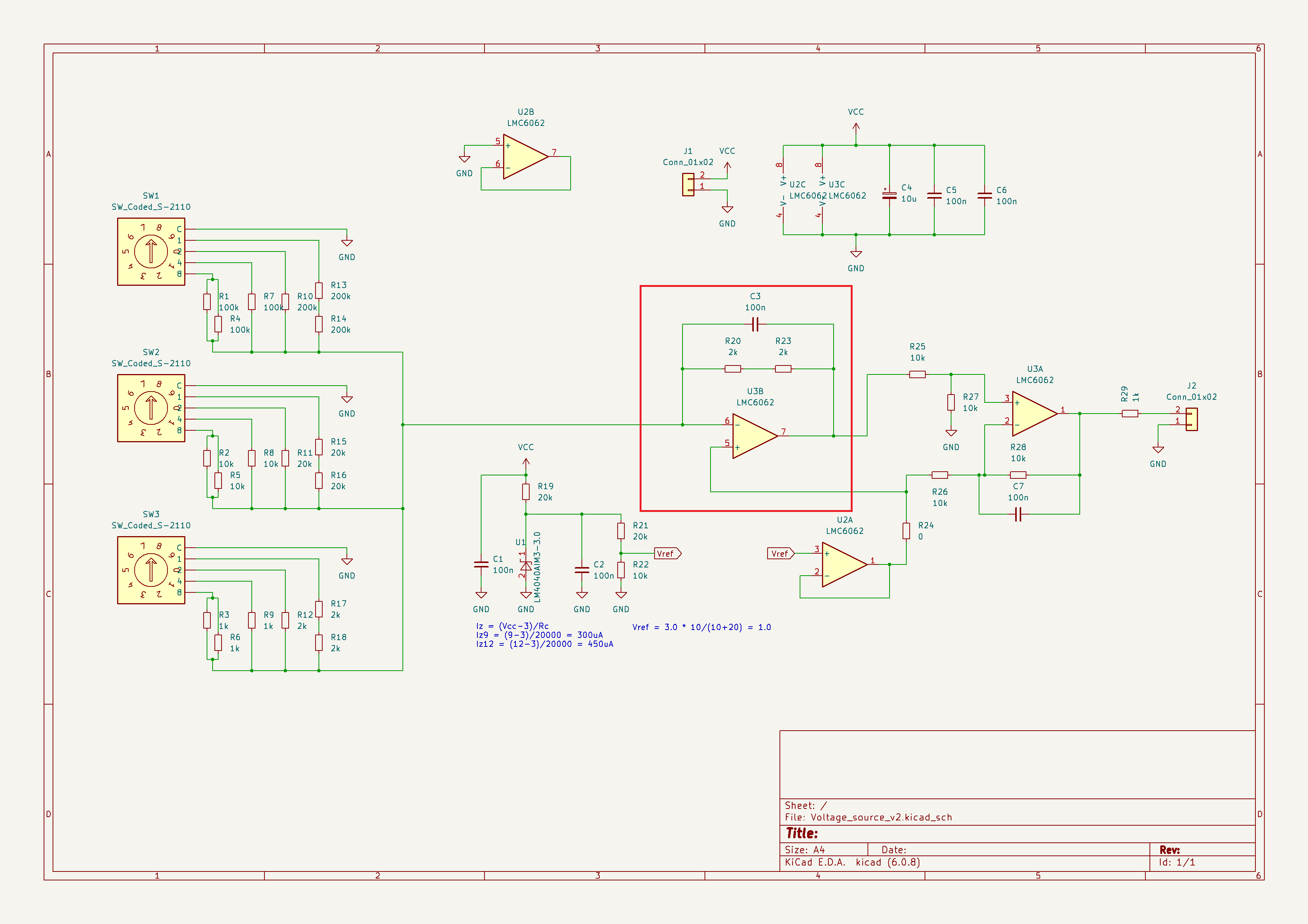
This is the part of the circuit where the desired voltage is generated.
The way it works is the following.
The voltage on the non-inverting input (pin 5) of the operational amplifier U3B is kept at a constant level of 1V coming from the reference voltage source.
Since the operational amplifier U3B has a negative feedback (provided by R20, R23, C3) it will effectively try to maintain the same voltage on both of its inputs, therefore the output of the operational amplifier will have the voltage value sufficient to keep the inverting input (pin 6) at 1V.
Now, let us go to the part where the output voltage gets set.
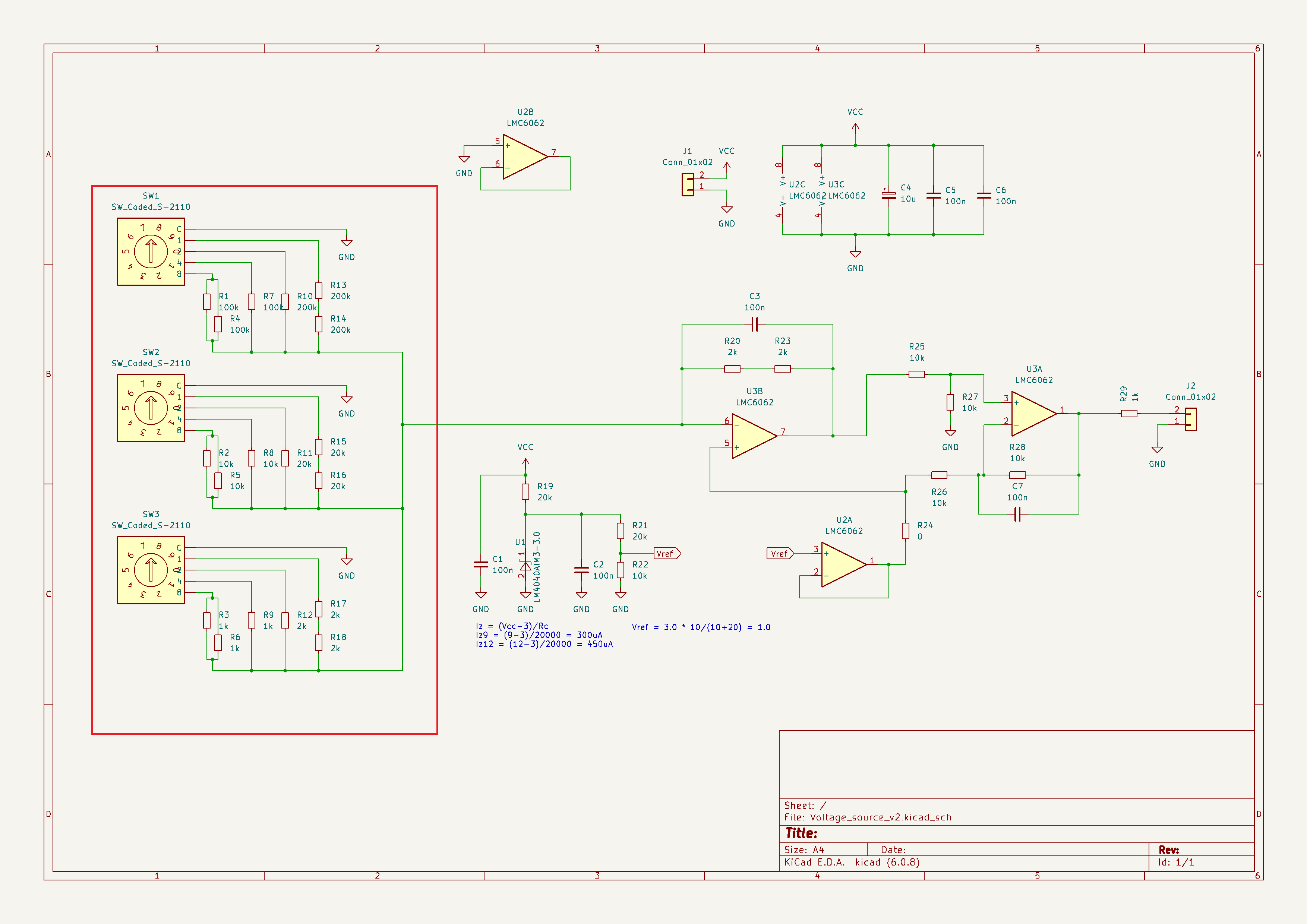
The non-inverting input of U3B is connected to ground by a set of switchable resistors.
There are 3 separate BCD (Binary Coded Digit) switches type Copal S-2110A forming three sections (1, 2, 3), counting from bottom to top.
Let us have a closer look at a single section (section 1) with its set of resistors.
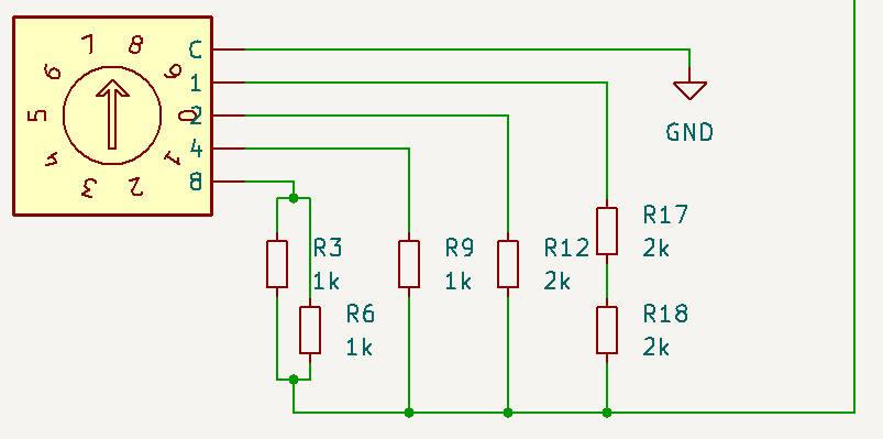
The switch can be set in any position, ranging from 0 to 9. The outputs are coded in binary as 1, 2, 4 and 8. For each position the position value is encoded in binary and the outputs with proper weights (1, 2, 4, 8) are either connected to common or left floating, depending on the version of the switch. The switches i use in the circuit are of the variety that makes the connection for the proper coded binary positions:
- for position 0 no outputs are connected to common terminal,
- for position 1 the output marked as 1 is connected to the common terminal,
- for position 2 the output marked as 2 is connected to the common terminal,
- for position 3 the outputs marked as 1 and 2 are connected to the common terminal,
- and so on...
In the circuit, the common terminal is directly connected to ground, so the switch effectively connects the resistors to ground or leaves them floating.
The values of the resistors are selected in such a way, as to provide a set of binary set of values (500 Ohm, 1000 Ohm, 2000 Ohm, 4000 Ohm) = 500 Ohm * (1, 2, 4, 8).
This means, that in order for the U3B to maintain 1V on its non-inverting input, the sufficient current must flow through the resistors that are currently connected to ground. The current has to flow through the series connection of R20 and R23 (2k + 2k = 4k) as well, since it is the output of the opamp that must provide this necessary current. We can safely neglect the input bias current of U3B, since it is a few orders of magnitude smaller (in the range of 0.1 nA) than the current considered. Therefore the output of the U3B amplifier has to be at the voltage shown in Table 1 (still we consider only one switch), taht can be easily calculated as: where I_R is the current through the resistors connected to switch.
You can also think about this part of a circuit (Figures 4 and 4a) as a non-inverting voltage amplifier with the gain set as
and the input voltage being 1V. It is just the same.
Table 1. Resistance, current anf voltage values for different positions of one switch
| Switch position | Resistance to ground [Ohms] | Total current through the resistors [mA] | Voltage on the output of U3B [V] |
| 0 | infinite | 0 | 1 |
| 1 | 4000 | 0.25 | 2 |
| 2 | 2000 | 0.5 | 3 |
| 3 | 1333.333 | 0.75 | 4 |
| 4 | 1000 | 1 | 5 |
| 5 | 800 | 1.25 | 6 |
| 6 | 666.667 | 1.5 | 7 |
| 7 | 571.429 | 1.75 | 8 |
| 8 | 500 | 2 | 9 |
| 9 | 444.444 | 2.25 | 10 |
All the resistors used in part from Figure 4 and Figure 4a should be precise, so I use 0.1% ones here.
The capacitor is just a 100nF generic X7R ceramic capacitor to limit the bandwidth of the amplifier.
All three sections from Figure 4a work in the same way, only the currents are decreasing by the magnitude of 10, since the resistors have values from 5k to 40k (section 2) and from 50k to 400k (section 3), so the output voltage of U3B will vary between 1.0 and 1.9V for section 2 and between 1.00 and 1.09 for section 3.
When currenst of all 3 sections add up, the output voltage of U3B will vary between 1.00 and 10.99V with a step of 0.01V (ideally).
Therefore, the voltage (in volts) of the output of U3B follows the equation:
When, for example, the switches are set to the positions 5, 3, 7, the voltage at the output of the U3B will happen to be:
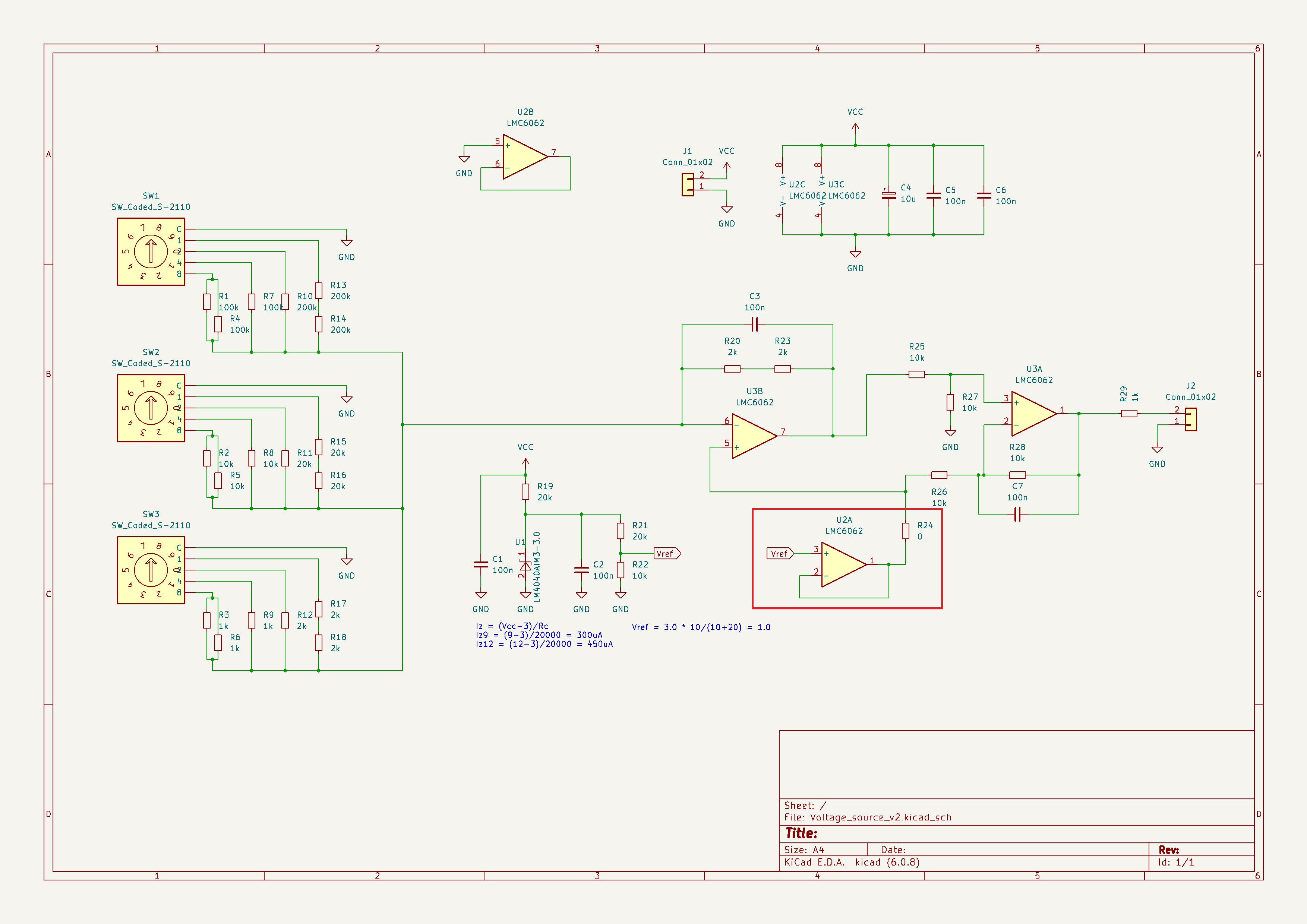
Difference amplifier
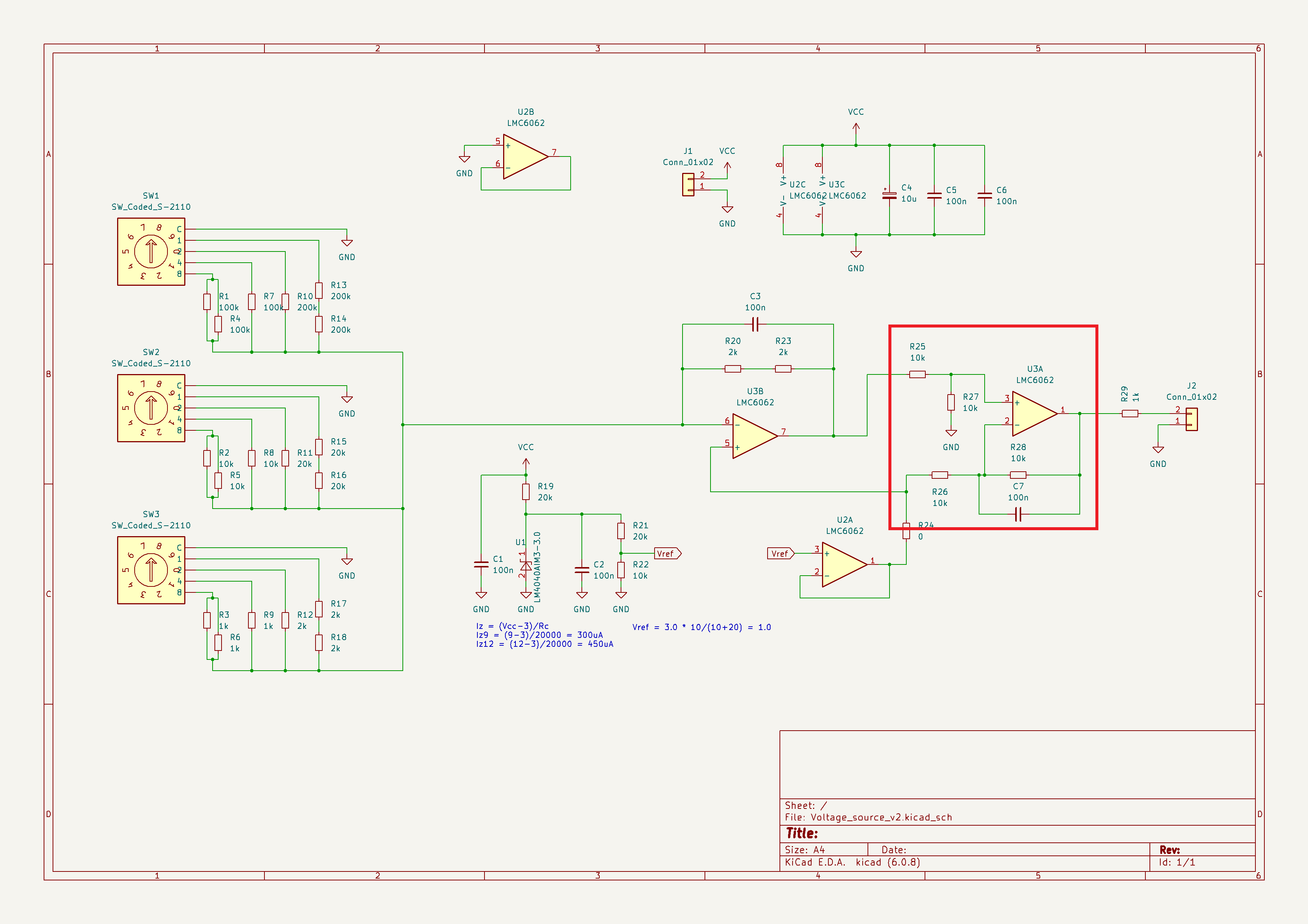
In order to get the voltages back within the range of settings of BCD switches, that is 0.00V to 9.99V, the voltage on the output of the U3B needs to be decreased by 1V. This is done in the difference amplifier. All the resistors have the same value (10k) and since precision is important here, they should have the tolerance of 0.1%.
The output of the U3A is
This voltage can be fed to the output through the resistor R29 that serves the purpose of providing some kind of separation between the output of the operational amplifier and any possible load (for example, capacitive) that can be encountered by the circuit. It can be replaced by a short if necessary.
The U2B amplifier is left unused (confgured as a buffer with input grounded to limit the supply current) for possible future extension.
I mean to use the circuit with a breadboard, therefore the connection with loose wires is sufficient for now, until further extensions are designed.
Advantages
The circuit surely has some good features
- For sure it is simpler than Kelvin-Varley divider
- Using components that are possible to source easily
- Its accuracy seems to be OK
Shortcomings
The shortcomings of the circuit include the following:
- The output voltage is limited by the suply voltage. If it is powered from 9V, the maximal output voltage would be a bit below 8V (approximately 7.99V). This is due to the fact that the output of U3B needs to be 1V above output voltage. While setting higher value on the switches is possible, the output voltage will not follow the settings and there will be no warning. The fourth operational amplifier, left unused, might provide some kind of warning, but since it would not be accurate without adding another amplifier, I did not include any kind of warning LED in the current circuit.
- Also for low output voltages, below 0.1V, some errors may be observed due to the vicinity of the lower rail of supply voltage of operational amplifier. Although it is rail to rail, it may not be able to pull the output voltage down to exactly 0V.
- The switches used are specified for 10000 cycles. They will wear out eventually and will require replacement.
- The current consumption depends on the output voltage. For the highest output voltage of 9.99V, the circuit itself consumes above 3mA just for resistor currents. The solution would be to use higher valued resistors, but rising their values 10 times (other multiplier is impractical, since it would need difficult to obtain resistance values) would mean that the third section of switches would work with resistors in the range of megaohms. 2M Ohm precise resistors are not that common.