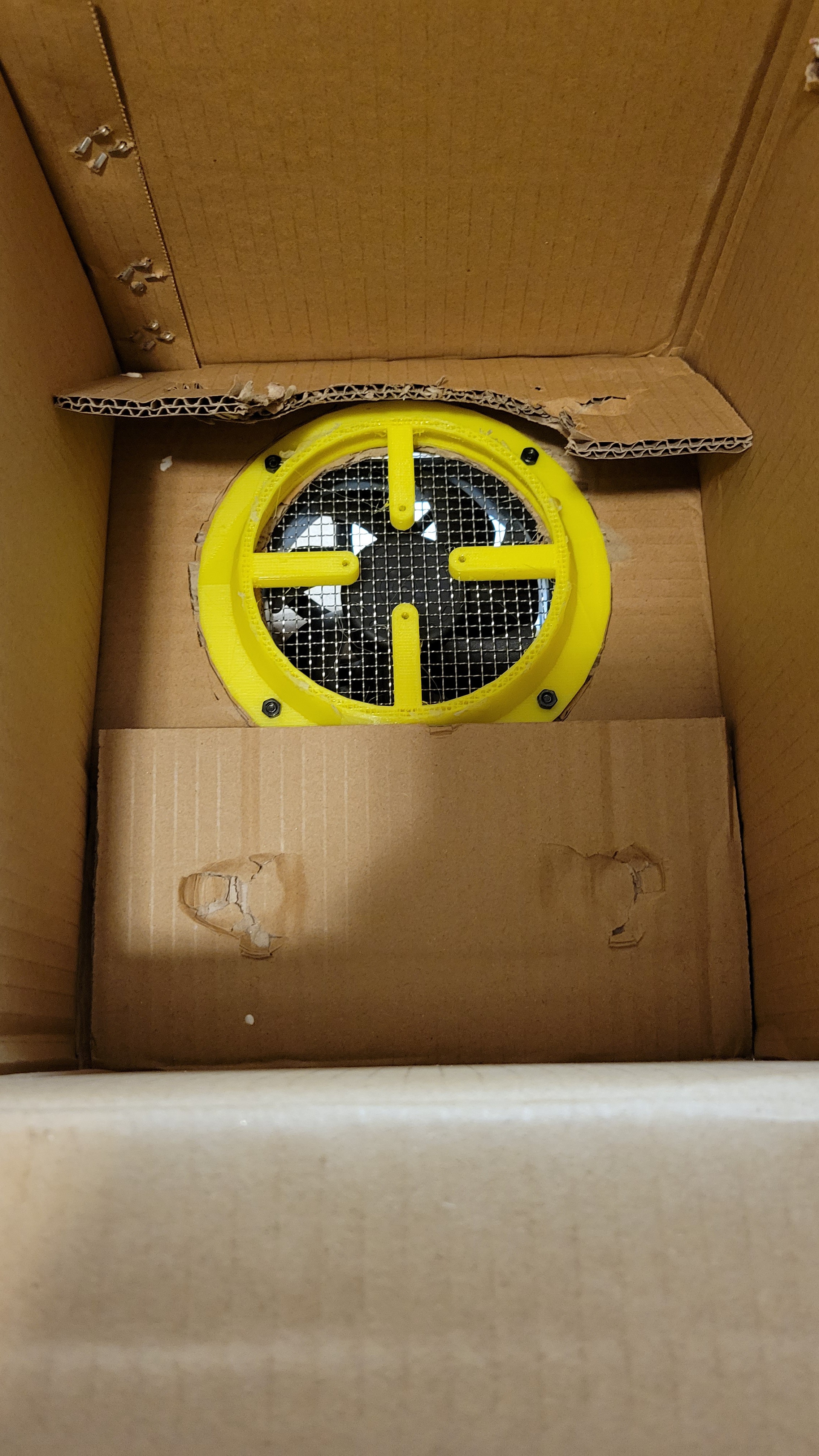
I suspect that last time the problem was shielding that was too close. So this time, I used a box wide enough to not create capacitor between shielding and components.
Placed went to cool it down
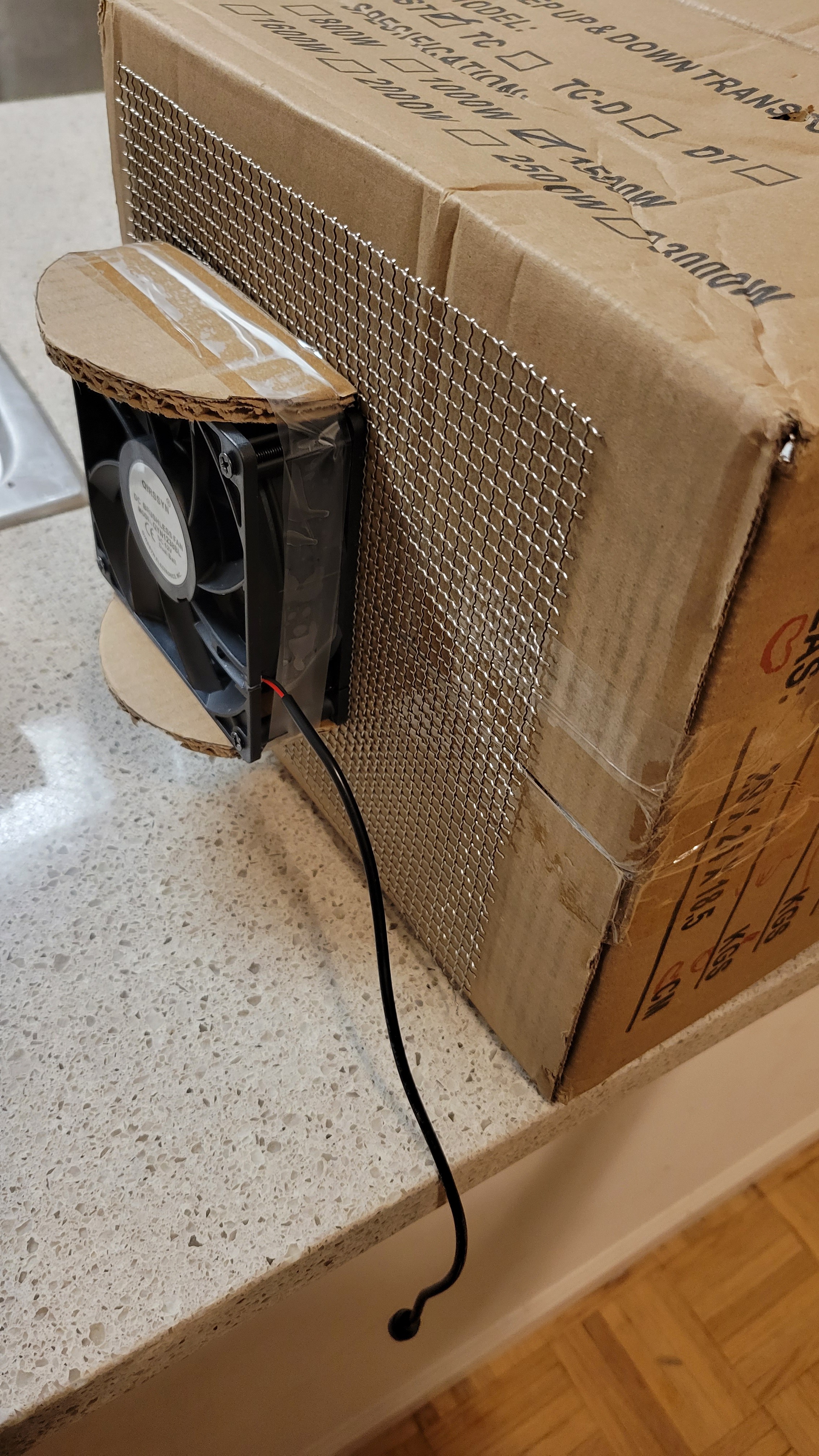
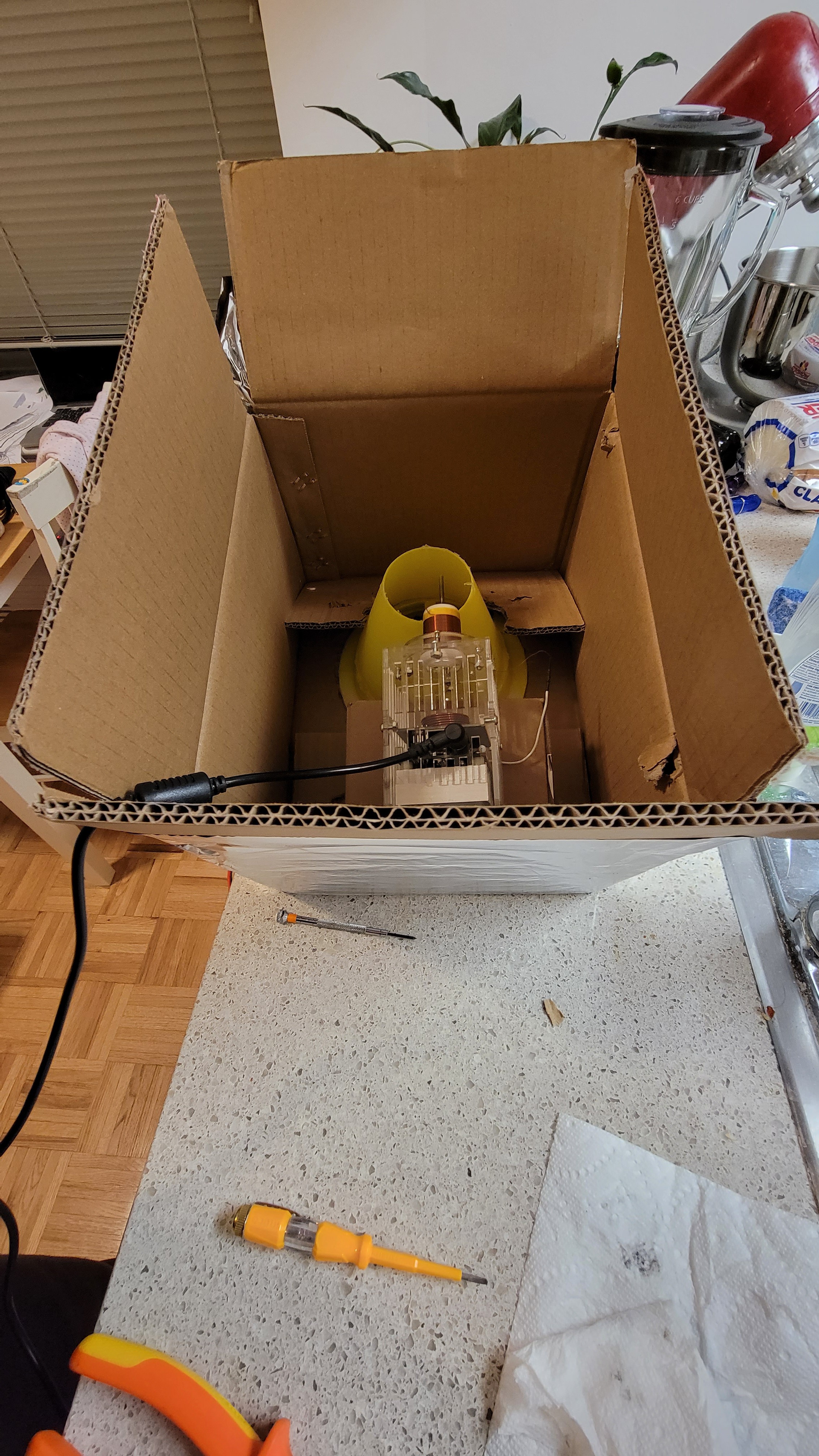
Made EM shielding using aluminum foil. Placed cone to concentrate air flow. And used more heat resistant Tesla coil
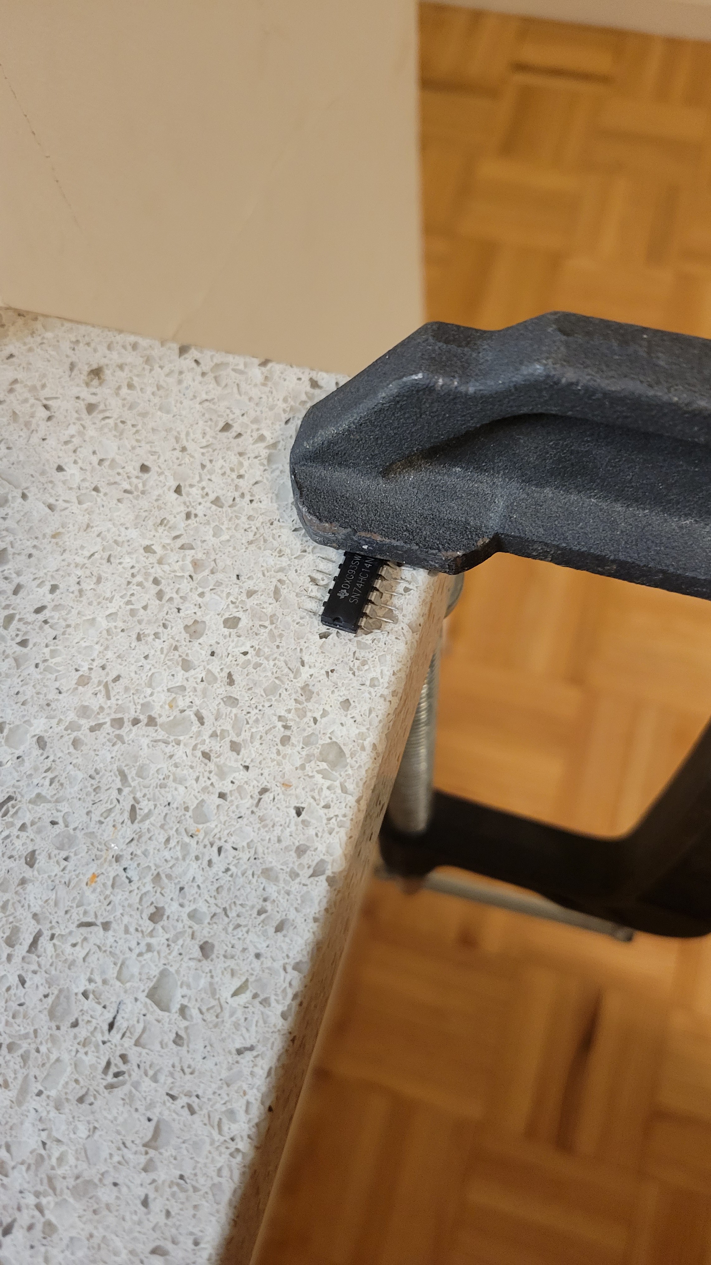
To speed up the process I've filed the IC package where I thought silicon should be (usually in the middle of the package)

Now for the fun part... PLASMA!!! That's a good place to warn everyone that you should NOT touch plasma with your hands or conducting material. Use ONLY shielded tools
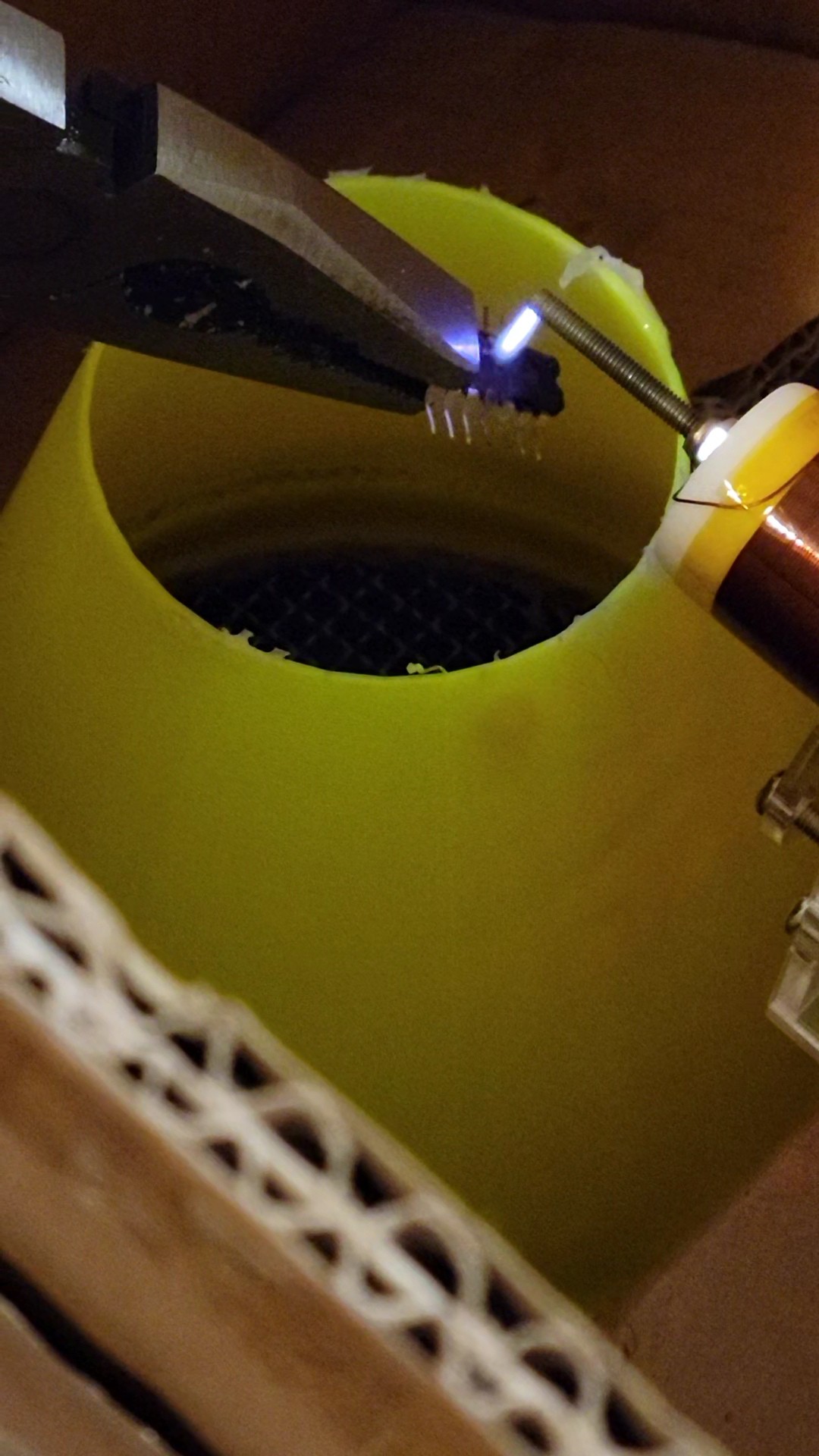
It still manual (I am testing some ideas how to make it automatic)
And the result:

In the middle you can see silicon. Now let's look on it under the microscope
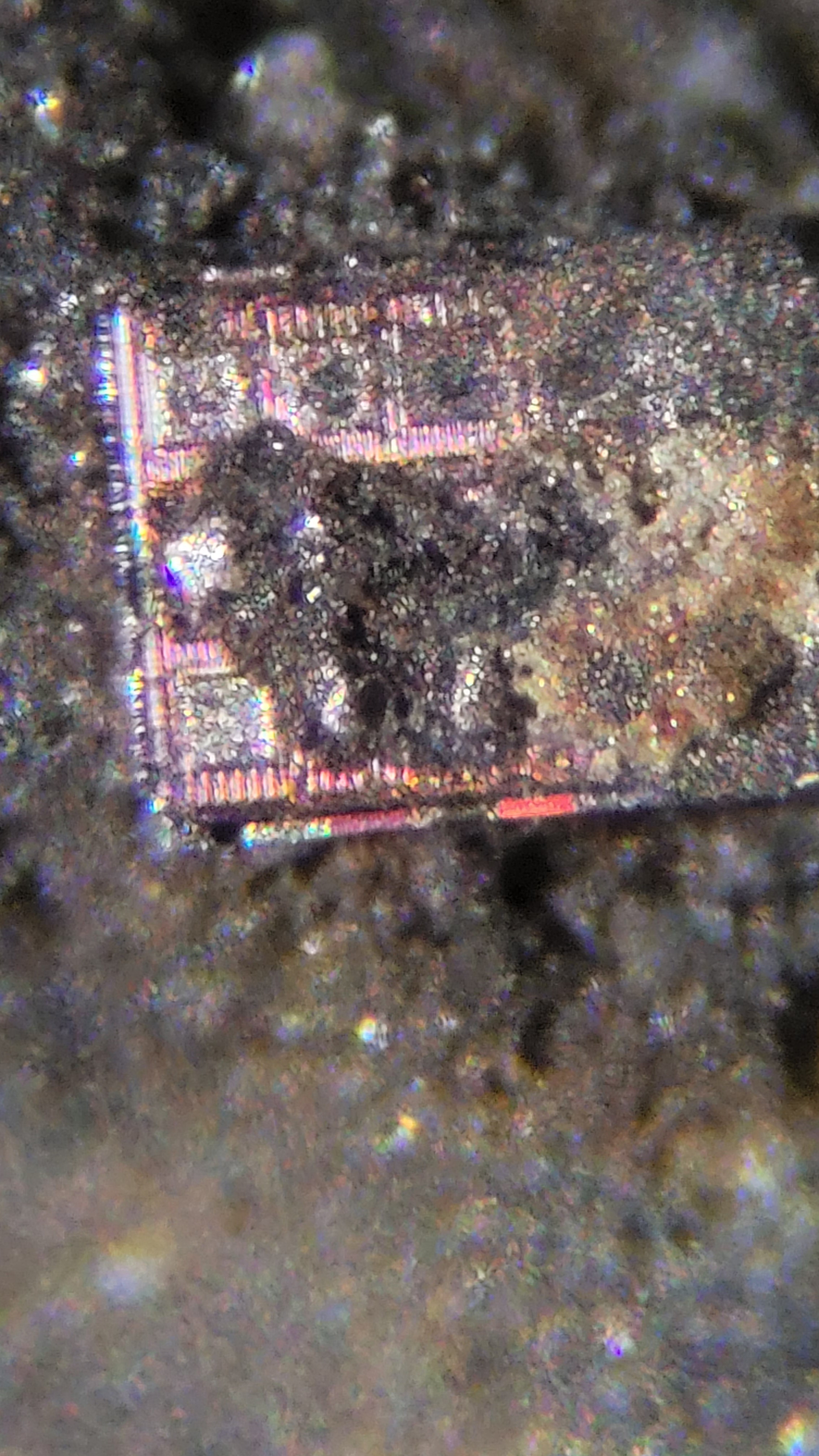
This time I got lots of residue left. I've tried to use more plasma but eventually silicon popped out and I was unable to find it. I guess I should use ultrasound bath next time.
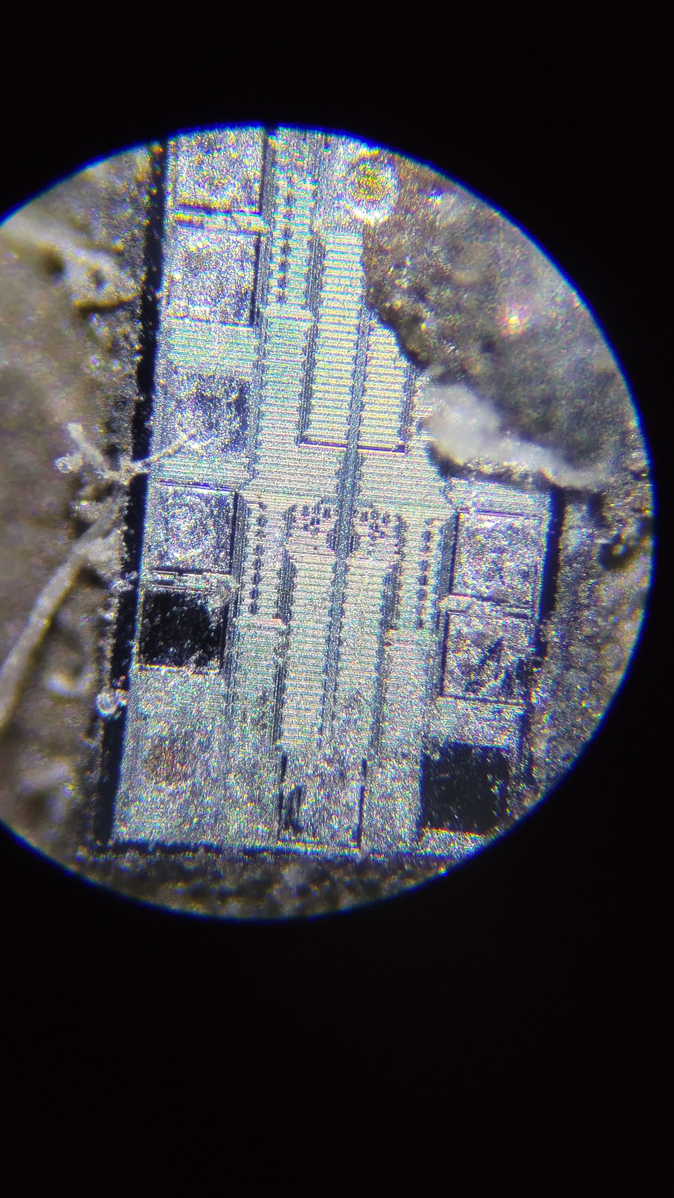
Here is another happily extracted silicon
Discussions
Become a Hackaday.io Member
Create an account to leave a comment. Already have an account? Log In.