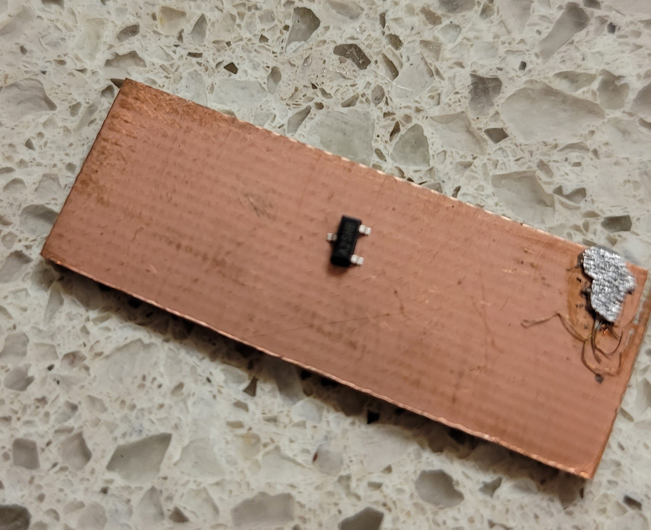
I got an interesting idea instead wasting time on removing upper layer of chip, why don't we use SMD version. It's really thin encapsulation, it will save tons of time. For standard one we could use laser or cnc to remove upper level.
So, here is our victim
This was not a good idea as the air passed near the PCB. The next trial I've used one with holes in it.
All clear fire down the hall:
It's looks like it missing the target but it's only because it really above. From side it looks ok.
Too close to plasma and it burned the PCB a bit.
So there is three parameters here the flame intensity controlled by voltage. Air flow speed controlled by fan speed and tray height.
Once all set you can just seat and drink well deserved tea.
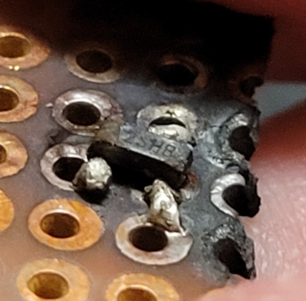
Instead of cleaning the burned residue with hands/tissue or screwdriver I've used ultrasound cleaner to gently remove all necessary and hopefully leave bonding wires where the are.
Fingers crossed, I will continue today. I prefer to take my time and do I right.
I had a problem with this setup, the blowing air can easily blow the plasma off and this apparently may damage Tesla coil. 😭
Discussions
Become a Hackaday.io Member
Create an account to leave a comment. Already have an account? Log In.