Doing the layout took a while as I had to make all the footprint libraries for this project and KiCAD had a bit of a learning curve with some of it's odd quirks! The layout was a bit tricky due to the clearances required and the low Z space I had inside my enclosure. I plan to fit everything inside of this enclosure:
http://uk.farnell.com/hammond/1591xxgsbk/enclosure-abs-black/dp/1877169

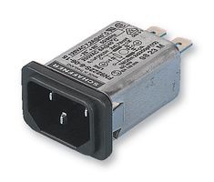
It is a tad expensive at £3.66 but should do the job nicely for a prototype. EMI filtering and connectivity was taken care by with:
http://uk.farnell.com/schaffner/fn9222sr-15-06/filter-15a-snap-in/dp/1190736
http://uk.farnell.com/schurter/6600-4120/outlet-iec-f-6600-10a/dp/2080452

The rest of the connectors are standard 0.1" header type ones. Layout is shown below:
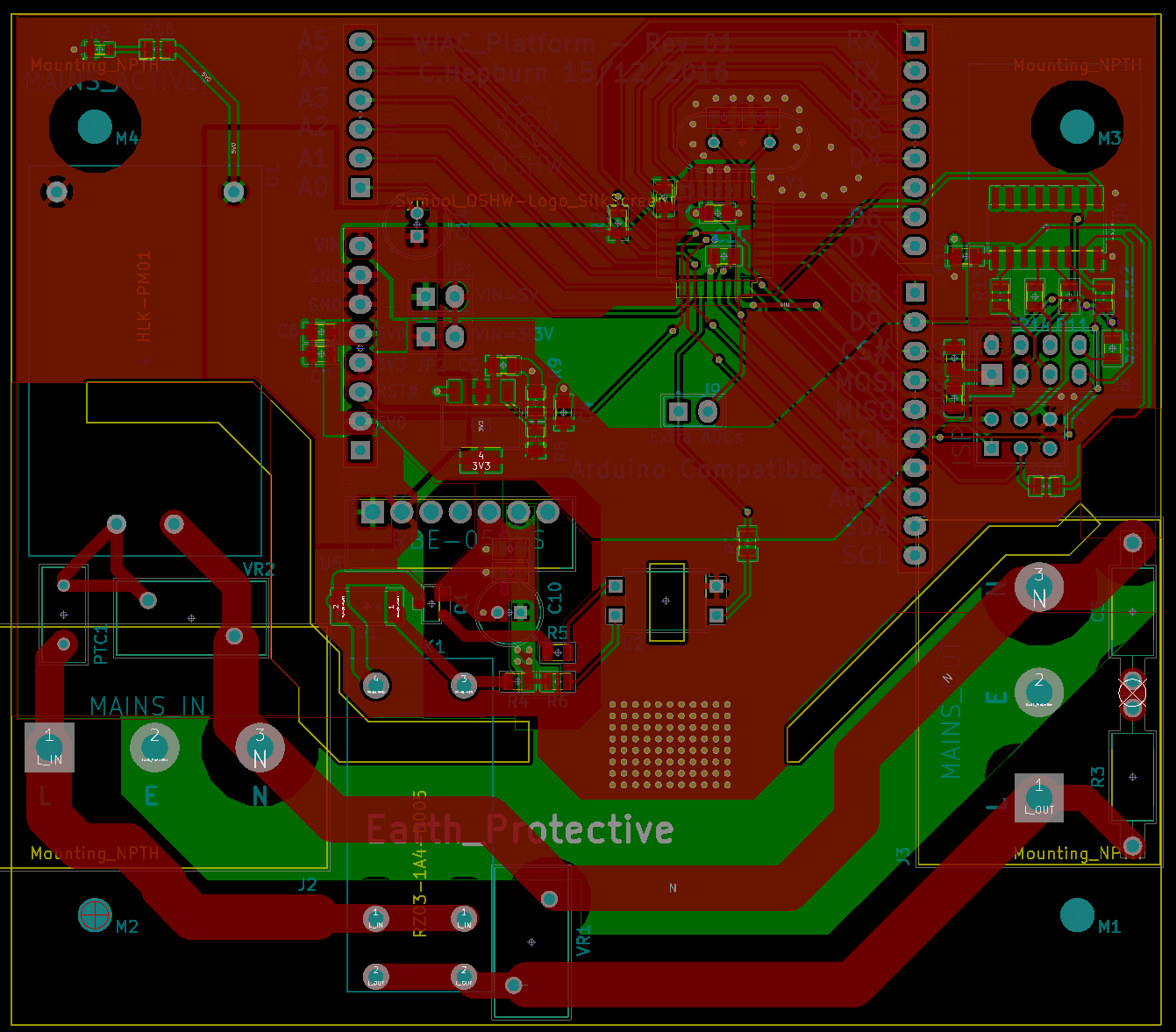
With this design it's very important that the live and neutral pins are mapped as shown in the layout to respect all the relevant clearances. Therefore this design is only suitable for keyed plug designs currently like we have in the UK. A reversable plug may not play nice with this revision.
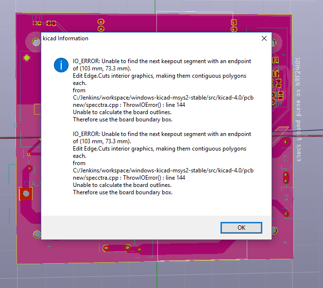
I also had this error come up as well, in case anyone else gets it, make sure to make sure there are no stray edge cut line objects hiding on top of another one. They won't be visible in the viewer but will give this error, so just find the culprit and delete it out.
Discussions
Become a Hackaday.io Member
Create an account to leave a comment. Already have an account? Log In.