Two posts ago I discussed the need for a faster optocoupler than the LTV-816S I was using before, and I mentioned the 6N136. Here’s why I selected that part:
- It was the first and most common result when searching for optocouplers on Digikey with transistor output, turn-on time less than 1us, and sorting by price.
- It’s a common component available from multiple manufacturers
- It was mentioned online as a faster alternative to slow phototransistor-based optocouplers.
- I probably have a tendency to see a part / get an idea and run with it, rather than evaluating all the options first. Which is kind of how I got sucked into this project in the first place...
Here’s the design I’ve settled on:
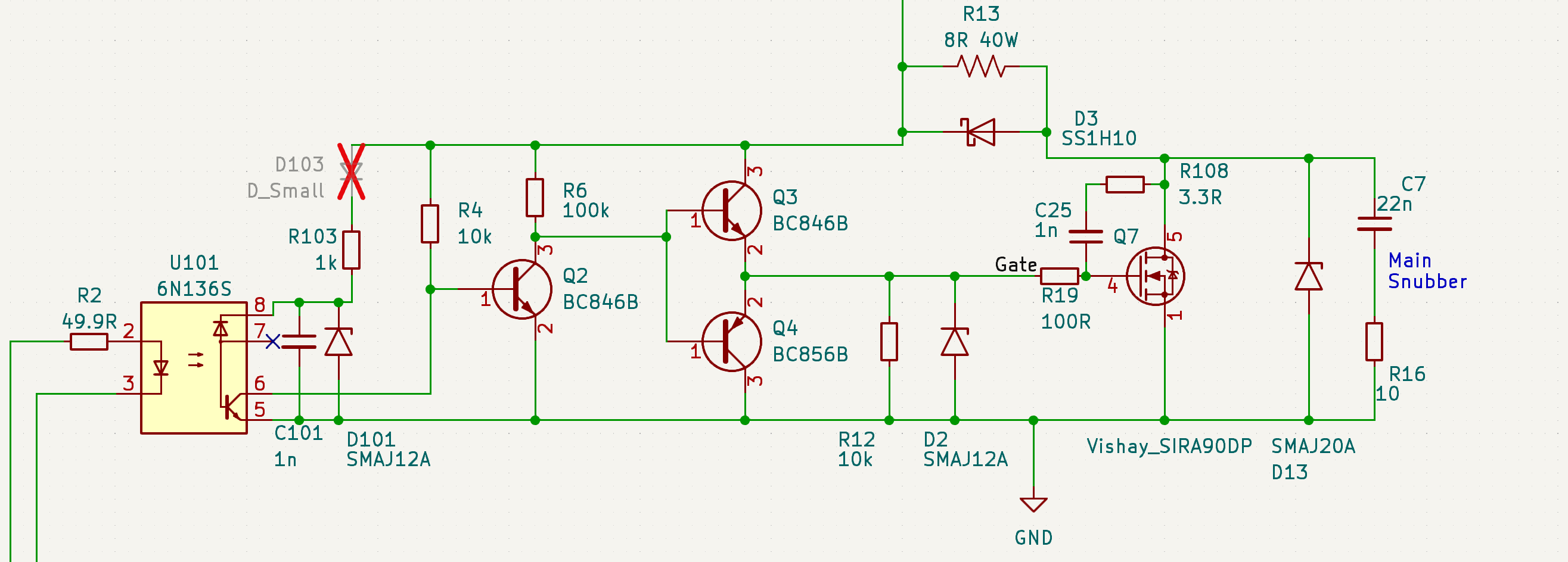
This has a few changes from the last design to accommodate the 6N136:
- It requires a higher drive current, so the input resistor is now 49.9R, combined with 49.9R series termination resistor on the control PCB, that should make the drive current 14-19.7mA depending on the Vf of each optocoupler.
- It has a max VCC voltage (pin 8) of 15V. Inductive spikes can cause the load stage input voltage to go up to 25V on a 12.2V input, only limited by the existing slew rate control circuitry and TVS diodes. I added a 12V TVS to VCC on the optocoupler with a 1k current limiting resistor to address this. This should clamp VCC to below 15V, and the supply current is minimal so the 1k is no problem otherwise.
- It needs a decoupling capacitor across its VCC and GND pins. I initially thought I might be able to get away without this, but testing showed it really is needed. I was getting an unusual oscillation of the gate drive on turn-on that went away when I touched the VCC pin, so the capacitance of my finger is all it needed in that case. The oscillation was most prevalent when switching higher currents, or when the cable inductance was increased.
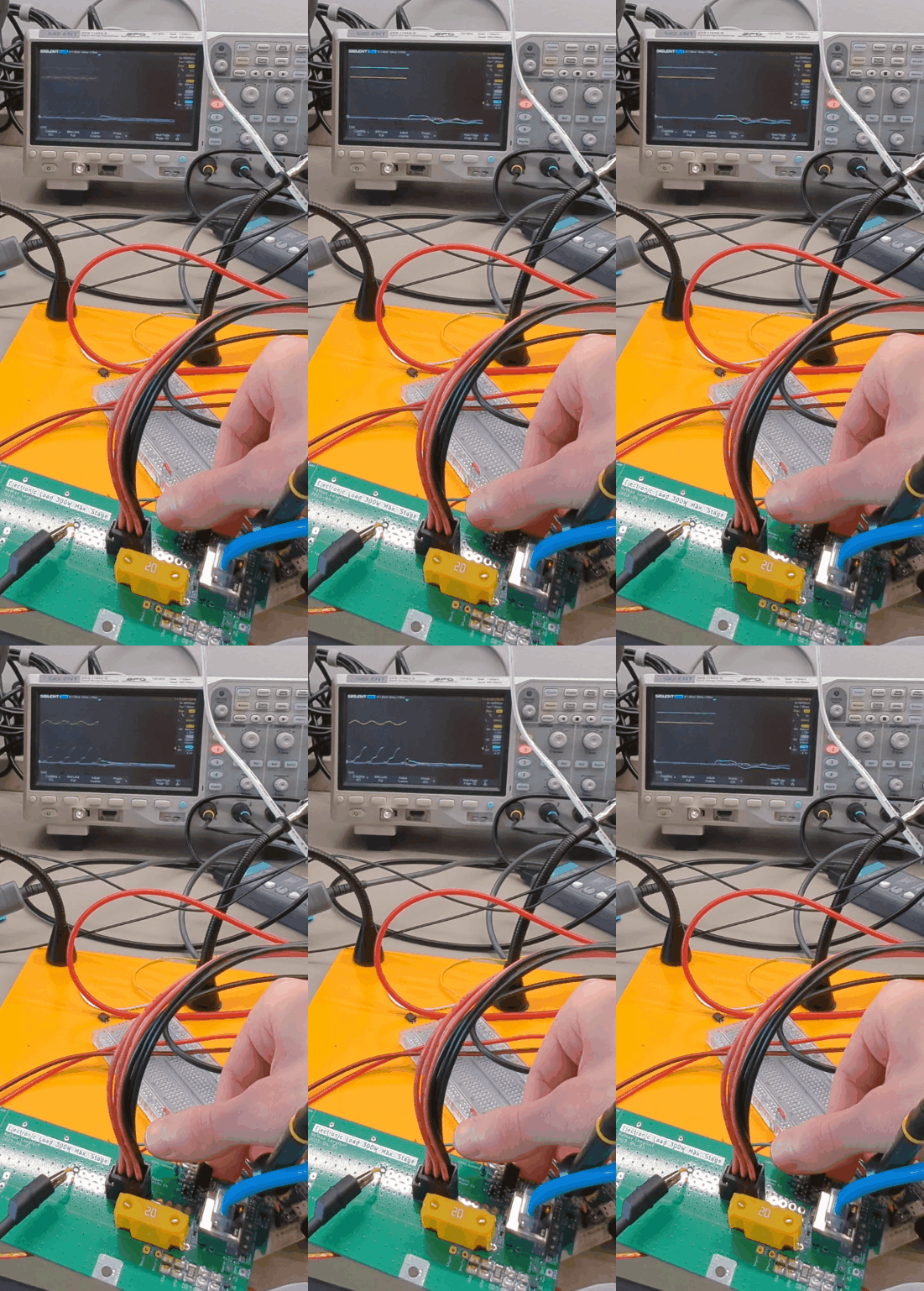
- The output pullup resistor was changed from 3.3k to 10k. Performance was satisfactory with the 10k, and it reduces the load stage quiescent current from the DUT to 1.3mA. This matters when there are 53 load stages.
- The pullup for the BJT inverter after the optocoupler was changed to 100k from 1k. This dramatically reduces the quiescent current. The resistor determines how much current the BJT push-pull driver stage can source during turn-on. However, for the turn-on transitions the gate driver speed doesn’t actually matter at all. The inductance of the load resistors is always the limiting factor, not the MOSFET turn-on speed. The turn-off transitions matter much more (and even then, only on the highest current 0.1R 122A load stages).
- I’ve added an optional diode in the VCC supply for the 6N136. I’ll probably just short this out but it leaves me the option to place it later. Any capacitance across the load stage supply is a large problem, because when the load stage turns off, the inductance of the load resistor and cables causes a voltage spike. This voltage spike causes any capacitor to get charged above the voltage of the DUT, so once the spike is clamped and the voltage comes back down, the capacitor is discharged back in to the DUT, forcing it to sink current. How much current can a power supply sink safely? I have no idea. I even wanted to eliminate the RC snubber across the MOSFET for this reason, but I don’t know of any other way to get rid of the ringing of the cable inductance and FET//TVS capacitance. The diode will prevent this added capacitor on the 6N136 from discharging this way, although the 1k resistor reduces the magnitude of the current going in reverse, even if the actual charge amount is the same.
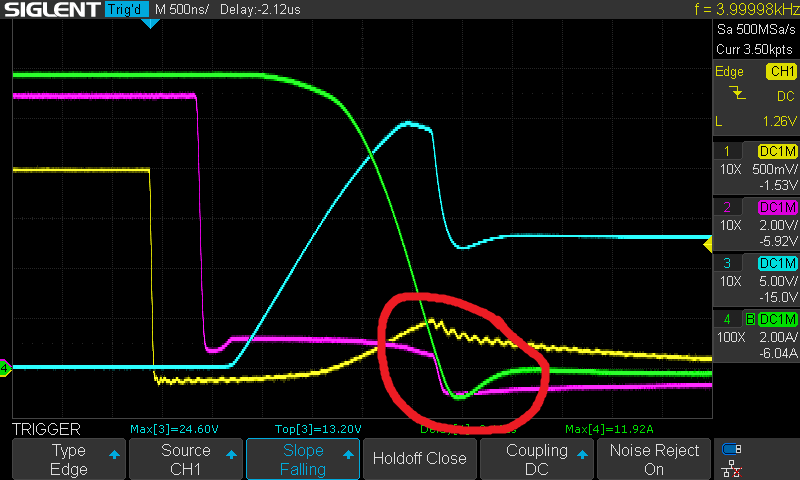
I’m relying heavily on simulation for the load stage design, so that was the next step after part selection. I know the simulation models won’t be perfect, but they are a whole lot better than my mental models!
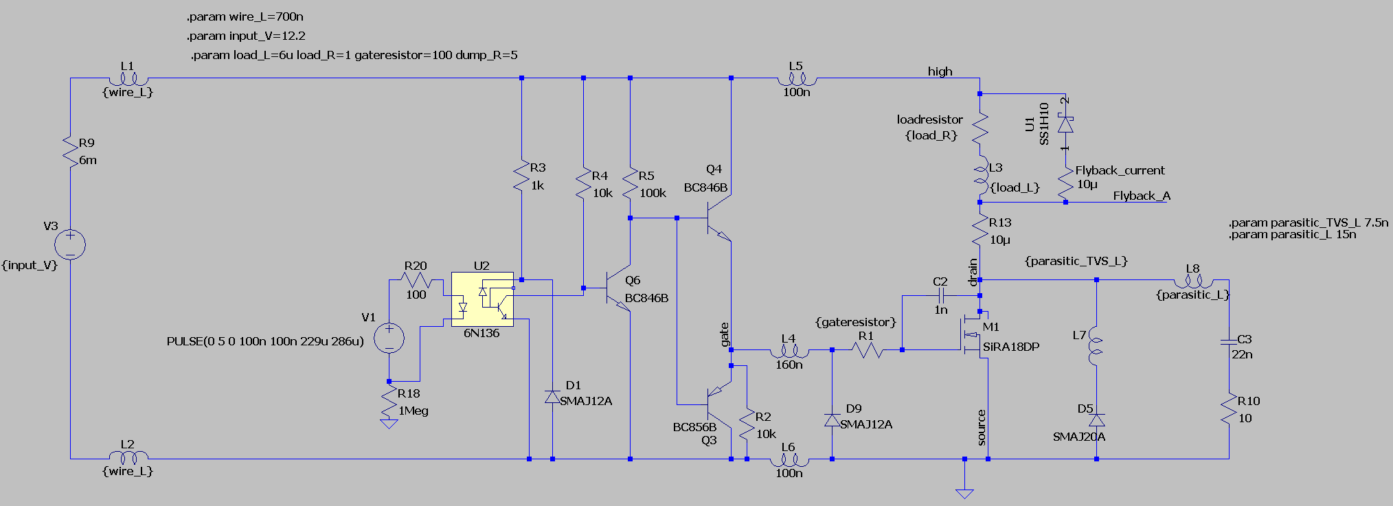
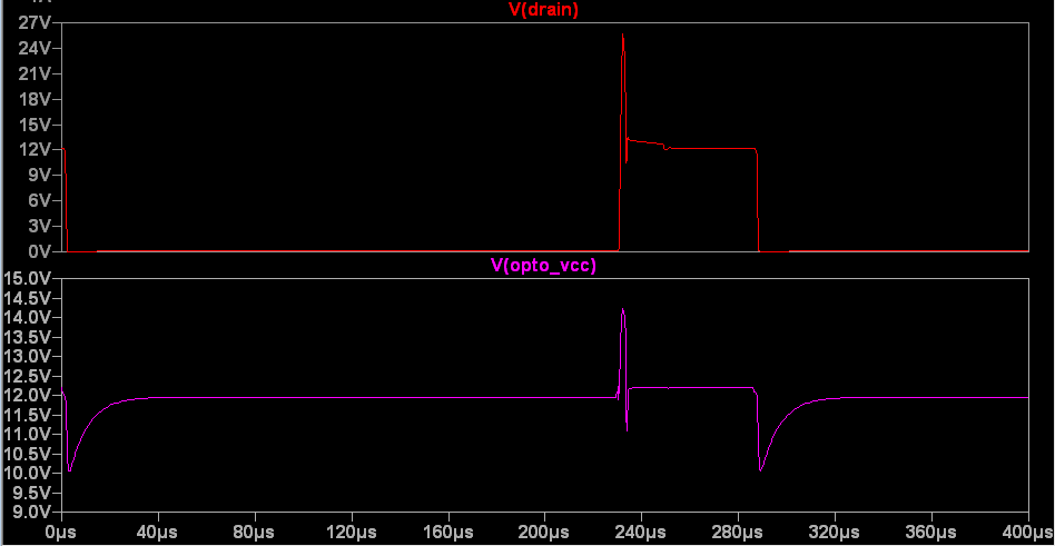
In the simulation I confirmed the VCC pin on the 6N136 stays under 15V. This isn’t a given when the load stage is switching a lot of current, bouncing around on the inductance of the cables.
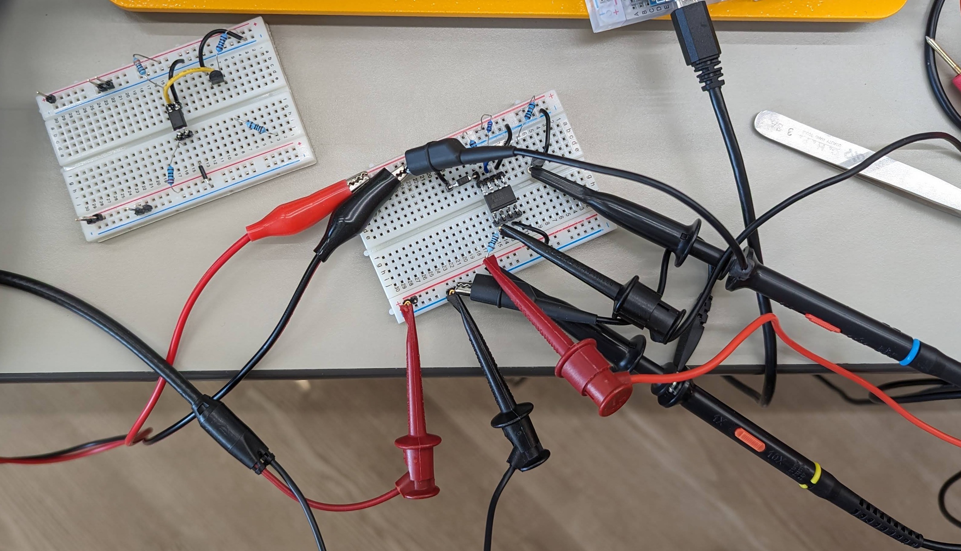
Once the new parts arrived, I mocked up a breadboard test before bodging it in to the load stage PCB I’ve been testing on.
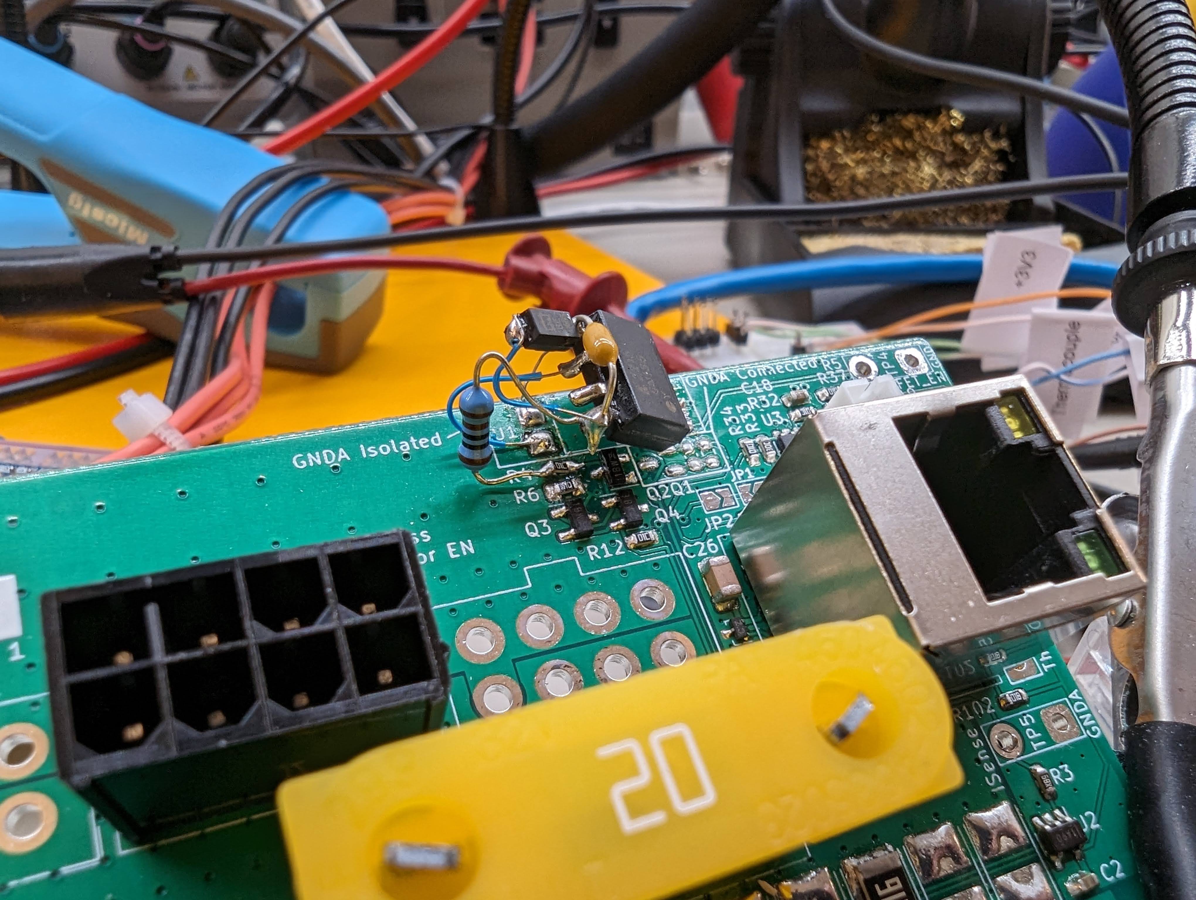
A bit of creative 3D soldering later and the operation was a success!
The results speak for themselves.
Breadboard Testing
Old optocoupler - LTV-816S with 2N3904 output inverter, 3.3k opto pullup, 1k inverter pullup
Turn-on delay: 1.40us
Turn-off delay: 30.36us
New optocoupler - 6N136 with 2N3904 output inverter, 10k opto pullup, 1k inverter pullup
Turn-on delay: 332ns
Turn-off delay: 572ns
New optocoupler - 6N136 with 2N3904 output inverter, 10k opto pullup, 100k inverter pullup
Turn-on delay: 2.73us
Turn-off delay: 560ns
(turn-on limited by 100k inverter pullup but this is fine)
Load Stage Testing
Turn-off delay with new optocoupler:
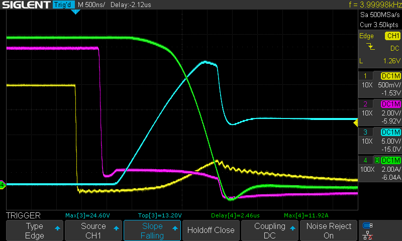
Turn-on delay with new optocoupler:
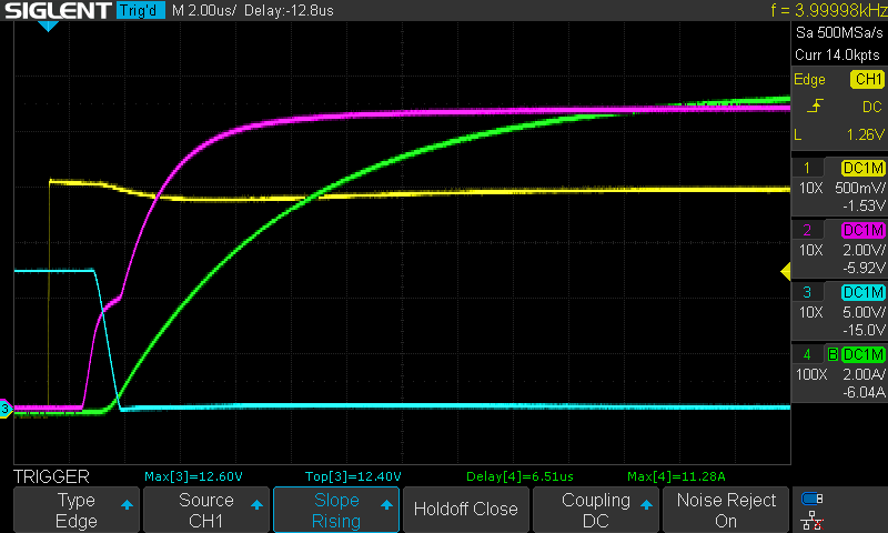
I consider going from 30us to 500ns a big success. On the upcoming new PCB revision, I might try reducing the 100k to something a little smaller like 47k to maybe reduce the turn-on delay a bit, because that won't increase the quiescent current that much. Other than that, I'm calling it good!
Discussions
Become a Hackaday.io Member
Create an account to leave a comment. Already have an account? Log In.