 Michael Gardi
As I add the Hall Effect Sensors to the PCB, I am trying to position them as consistently as possible to each other so that the readings from different sensors are the same. The first step is to bend the leads on the sensors in a uniform way. To that end I designed and printed a little jig.
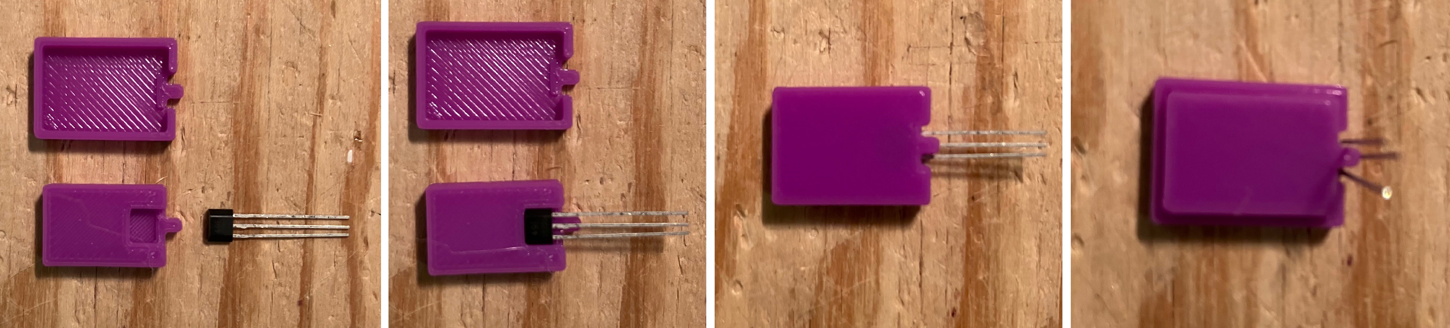
The sensor is placed into the indentation in the lower part of the jig, then the upper part is positioned on top as seen in the third photo above. With the sensor firmly in place, the jig is flipped and the three leads are carefully bent up 90 degrees.
To mound the sensor onto the PCB I first applied a small piece of two sided tape. (Apologies for the poor quality of the photos that follow.)
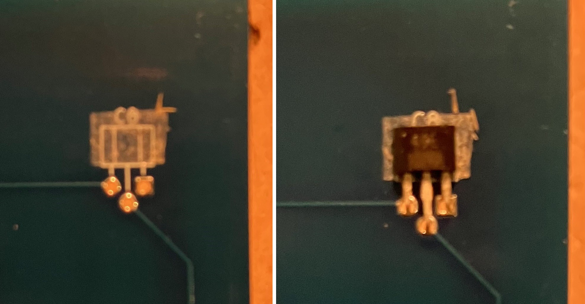
Then when the sensor is slid into place aligned with the square printed onto the PCB, it will be held securely so that it can be soldered.
Discussions
Become a Hackaday.io Member
Create an account to leave a comment. Already have an account? Log In.