 Chris
ChrisIn the last log we suffered through the very first revision of the CRAPi board! That whole experience really lived up to this board's namesake. Not surprised, just disappointed. The first two logs were retrospectives. Rather than just jumping into where the project is now I wanted to make sure I showed the last few months of design and trouble shooting. The board became more and more unreliable until it eventually refused to enter programming mode. Making stuff is hard!
Thankfully, this post now brings us firmly into the present. I had decided to cut my losses with Rev. 1 and focus on moving forward. I started Rev. 2 in the middle of February and "finished" the design around the middle of July, with time spent on the project ramping up exponentially once the semester was over. All told that's about 5 months worth of work. So here's what changed in that time:
Changes in Rev 2. of the CRAPi2040
- Pin Labeling
- Went back to traditional silkscreen but used a "knock-out," negative-space style.
- Improvements to the ProtoGrid
- Pin pads that should let solder bridges form more easily
- Better GPIO Access
- Vertically oriented pads for 20 mil spaced surface mount connectors
- More prototyping space.
- Thad Improvements
- Increased the diameter of the center hole to match diameter of common jumper wire
- Bread board jumpers can now be (hopefully) friction fit into the Thads and/or soldered
- Right Angled buttons
- Low profile buttons hang off the side of the PCB
- Allows for boot mode and resetting even when the board is upside down
- Route-able Power Pins
- Solder jumpers let you route 3.3V or VIN to either side of the board
- Independent of each other - 4 total configurations for max flexibility
- Configurable Power LED
- Lets you reclaim the red power-on LED for RGB usage
- A second BLUE LED attached to Pin 25
- Blue LED attached to GPIO 25, so default Pico blink examples are (almost) drop in.
- RESET and BOOT button breakout jumpers
- Solder jumpers to route the BOOT and RESET buttons to GPIO pads.
- Gives an optional, general purpose user button (which seems to be pretty rare!)
- Can reset itself (which I guess could be useful!)
- Castellated Holes
- Allows for use on a breadboard and as a module on a PCB
- No components on the back of the board so no cut out needed.
- QR Code Link to Documentation
- Quick access to pinout documentation because those labels are tiny!
- LiPo Battery Charging IC (!!!!!!!!!!!)
- Single cell LiPo battery charge and automatic switching circuity.
- On board indicator of charging status via a second RGB LED.
- Oh god why did I decide to add another IC to this design.
How's that for 5 months worth of work?
With all these changes it also meant that I needed to start routing completely from scratch. This time I decided to drop the trace width from 7 mil to 5 mil as well as the size of the vias. Just for my own sanity I also changed all the passive components on the board from 0402 to 0201. Some may argue that this was just exchanging sanity in the virtual world for insanity in the real world went I went to assemble the things.
Routing Comparison
All in all I'd say that I did a much better job routing this time around. My main focus was keeping traces on the top layer of the board and ground plane in tact on the bottom of the board. Just for fun I also made sure that to length match the traces going to the flash chip and the USB lines, mostly because I like how the squiggly lines look. Rev. 1 is on the left and Rev. 2 is on the right. Not bad right?
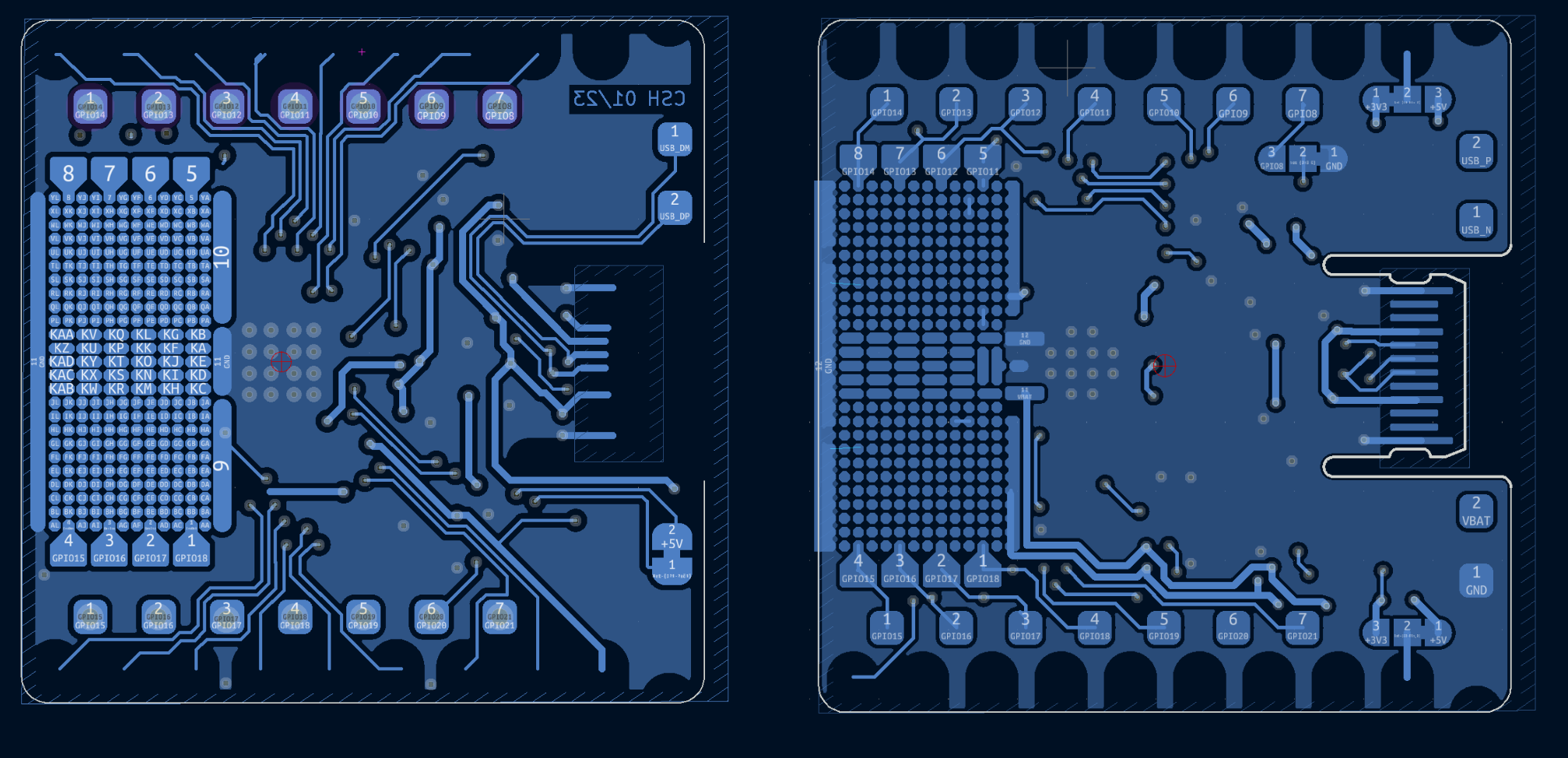
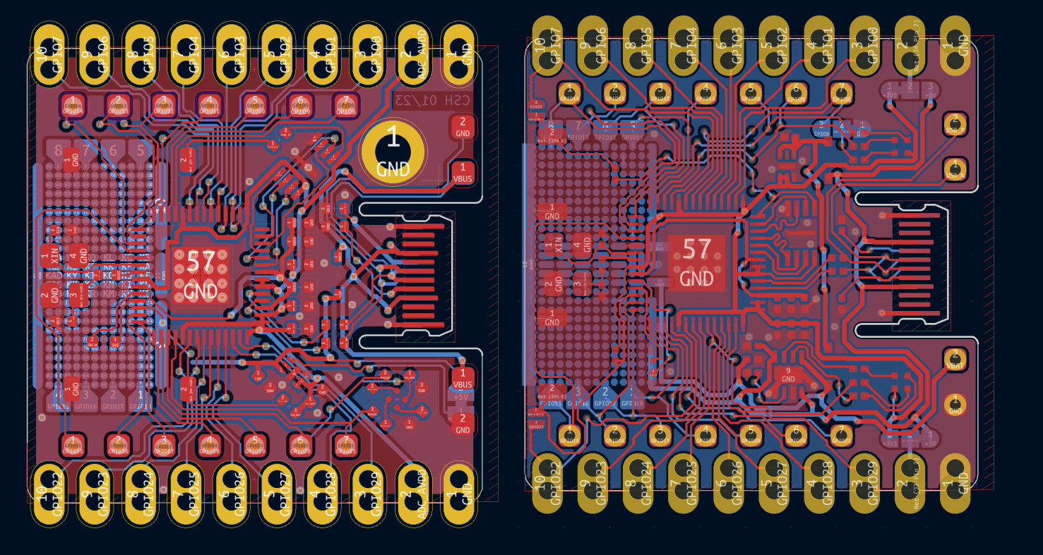 You can also see that I had to give up the mounting hole... I determined that all the new features would be worth give it up. The board doesn't have any components on the back side so you can always double side tape it down. I am also thinking about making some sort of carrier board that would solder to the Thads specifically to add mounting holes. So many ideas so little time.
 Cool Silkscreen HACKS!!!
Here are the obligatory KiCAD Renders. I spent a TON of time on laboring over the silkscreen labels on this revision. A huge peeve of mine is constantly looking up pin outs or counting headers to find the pin that I need. So instead of leaving that burden on the user of the board (future me), I put a half ounce more thought into my silkscreen labels.
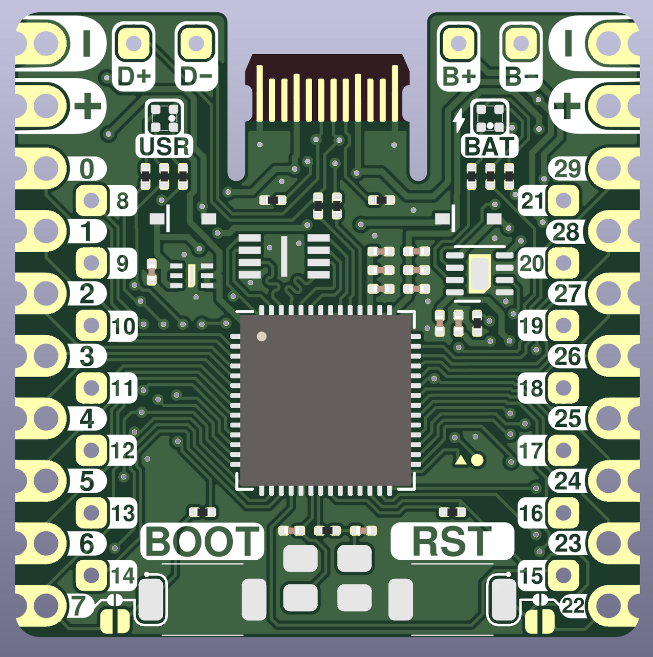
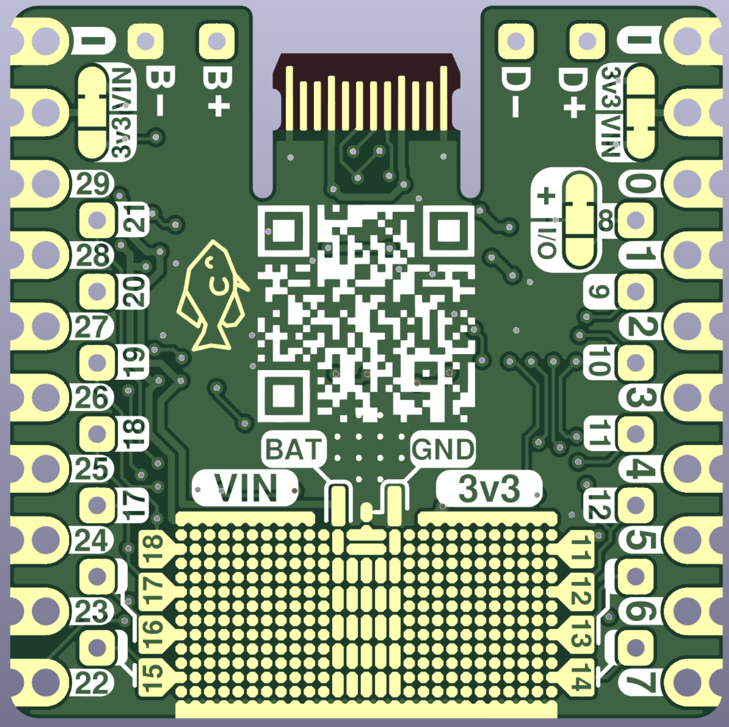
The real secret weapon to all of this was Inkscape. Pretty much part of the silkscreen was made in Inkscape, converted into a Path, then imported as a polygon on the sillkscreen layer. I would take a screen shot of the orthogonal 3D render, paste it into Inkscape, and then scale it to the dimensions of the board. That way I could create the silkscreen of one entire side in one shot, without needing to switch between softwares. When I was done, I only needed to perform a single polygon import.
You'll also notice that almost all of the text is in "knock out style." In other words, the text is written as negative space in the silkscreen. This is purposeful and is a great way to squeeze a little extra readability out of tiny silk screen labels. The advantages to the knock out style are two fold.
- Dark text with a light background is arguably easier to see and parse
- Imperfections / fuzzy edges are less impactful.
Point number one seems pretty intuitive, but I really had to think about point two. My explanation for this phenomenon is that it is much harder to deposit silkscreen precisely than it is to avoid depositing silkscreen. Additionally, such small amounts of silkscreen are most likely under deposited so the shape isn't really filling the outline that you want. This is actually advantageous for knock-out text because it "expands" the border of the text slightly.
Hopefully that makes sense.
RESULTS
Enough of this virtual non-sense, how did the boards turn out? Well, you tell me!
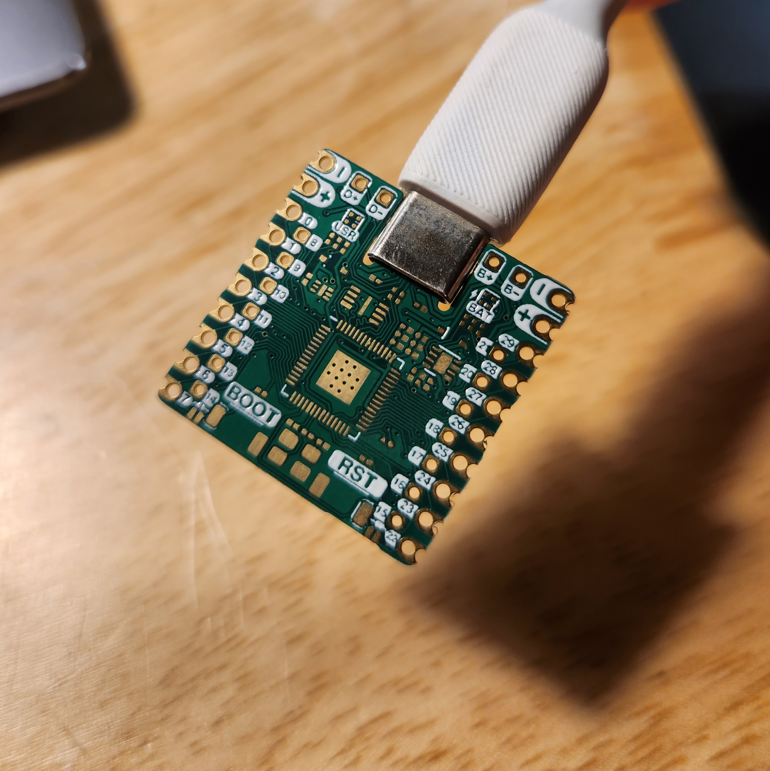
Oh, BABY! Isn't that just the most beautiful thing you've ever seen? After many long months, this thing turned out to be a work of art. Also notice what it's connected to!!! That's right
THE BOARD THICKNESS WAS CORRECT!
But I didn't want to get my hopes up too much. I figured that a good way to test if the pins of the board were making contact where they were supposed to was to cover the connector with dry erase marker, connect it, and see where the marker had rubbed off.
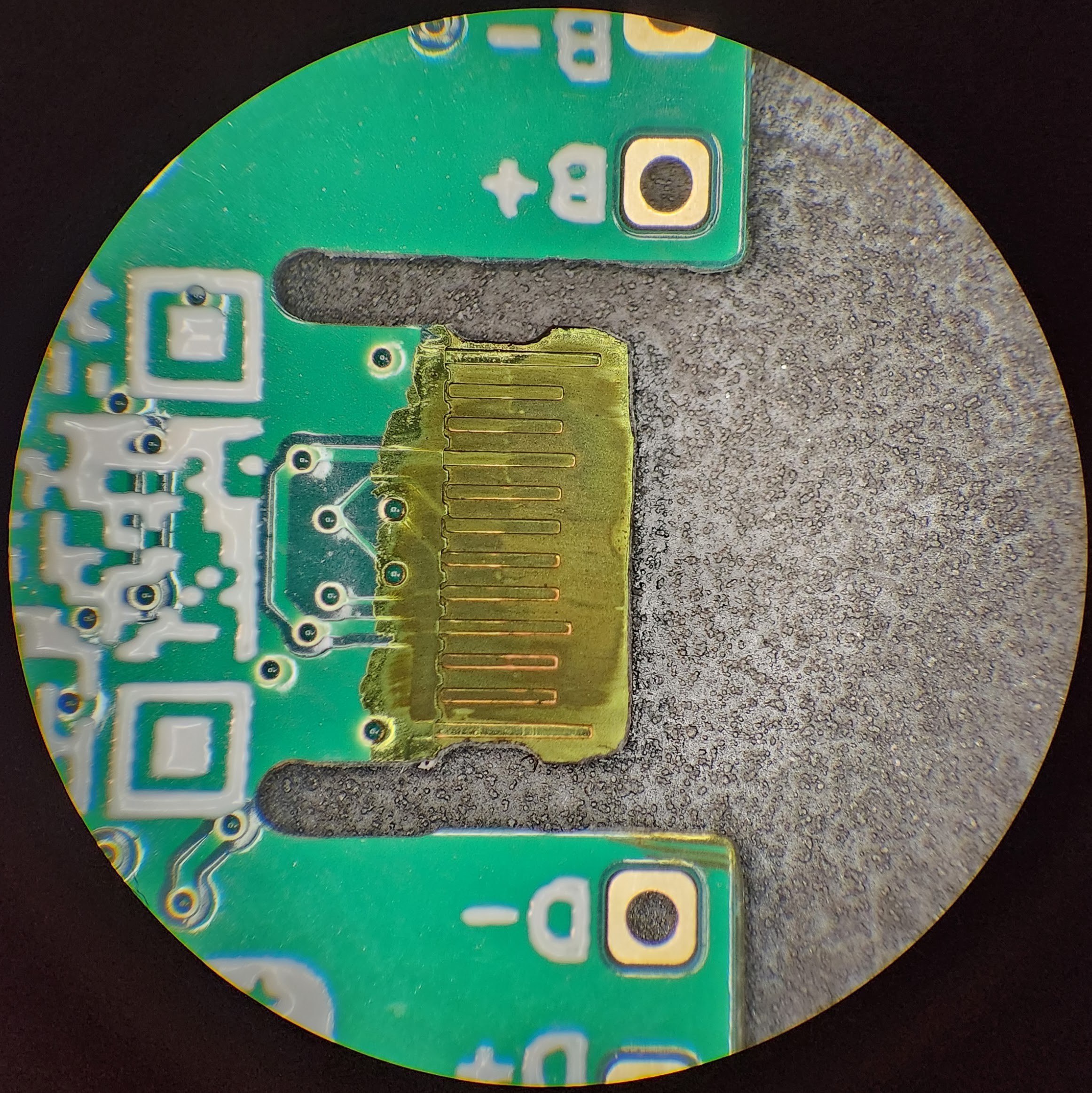
Sure enough, after connecting and disconnecting just a typical USB-C cable the results were almost perfect. The Ink was missing was perfectly removed from right on top of the pins. The pins inside the connector had made contact and wiped away the ink. The two outer most (and longest) are ground pins which makes sense. The next two inner most, and slightly longer pins are the D+ and D- pins for the USB.
 You'll notice that there is a bonus 5th pin that has been wiped clean as well. Initially I thought that the pins were making uneven contact which is why some some of the pins were wiped and others were not. Then I looked inside my USB-C cable and oddly enough not all of the contacts inside the connector are populated. So everything looked exactly how it was supposed to! The ink also reveals that the contacts are making contact with the PCB a reasonable length down the trace.
 I don't see a reason why this connector can't sustain a USB connection given the positive results above, but we won't know for sure until I am able to program a fully assembled
HOW ABOUT THAT SILKSCREEN?
The other thing I was most excited to see was whether my theories on the knock-out style silk screen were valid. At first glance with the good 'ol eyeball it seemed like hypothesis was true: knock-out / negative-space labels can be more reliably read than their positive-space counter parts of the same size.
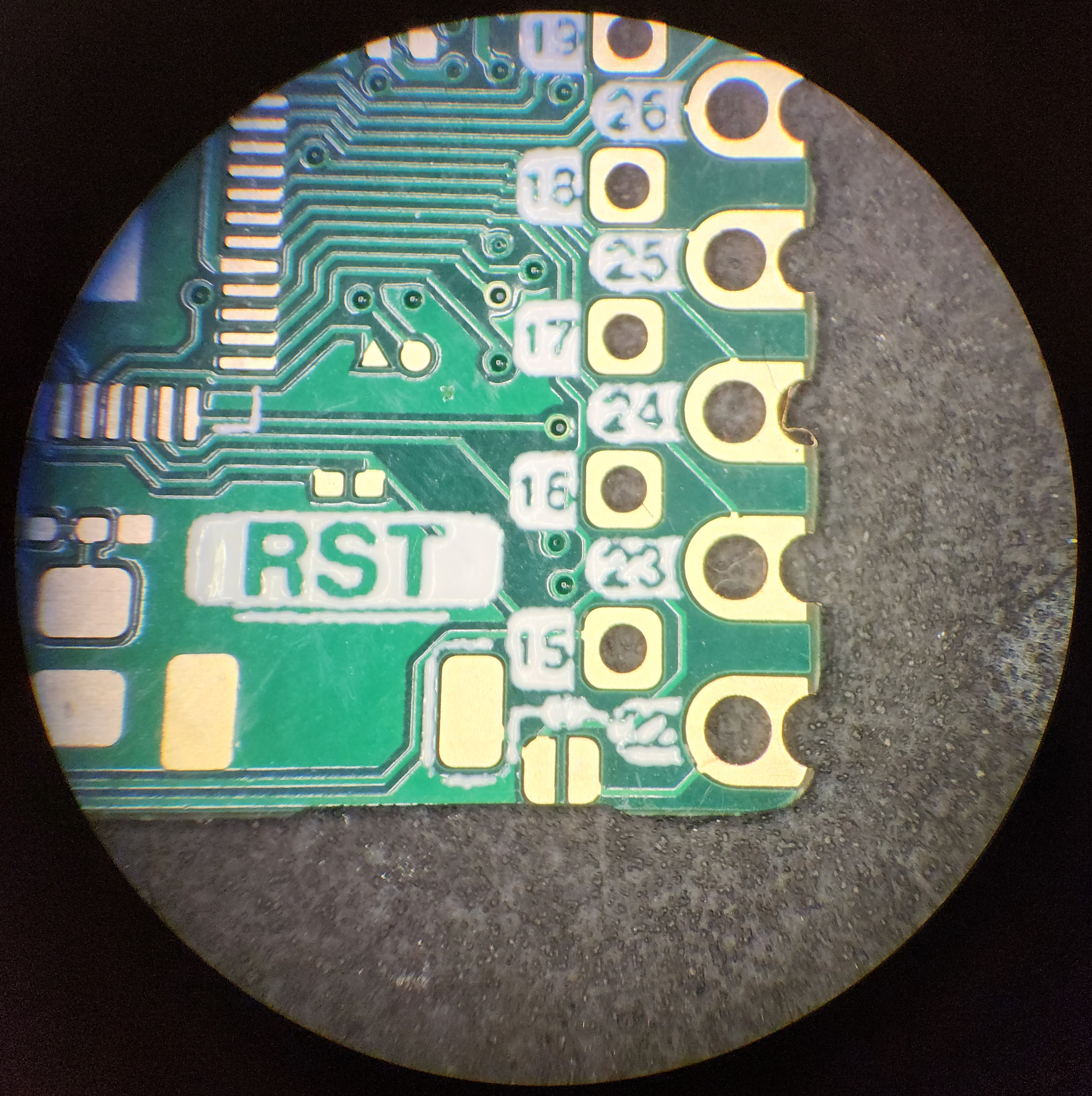
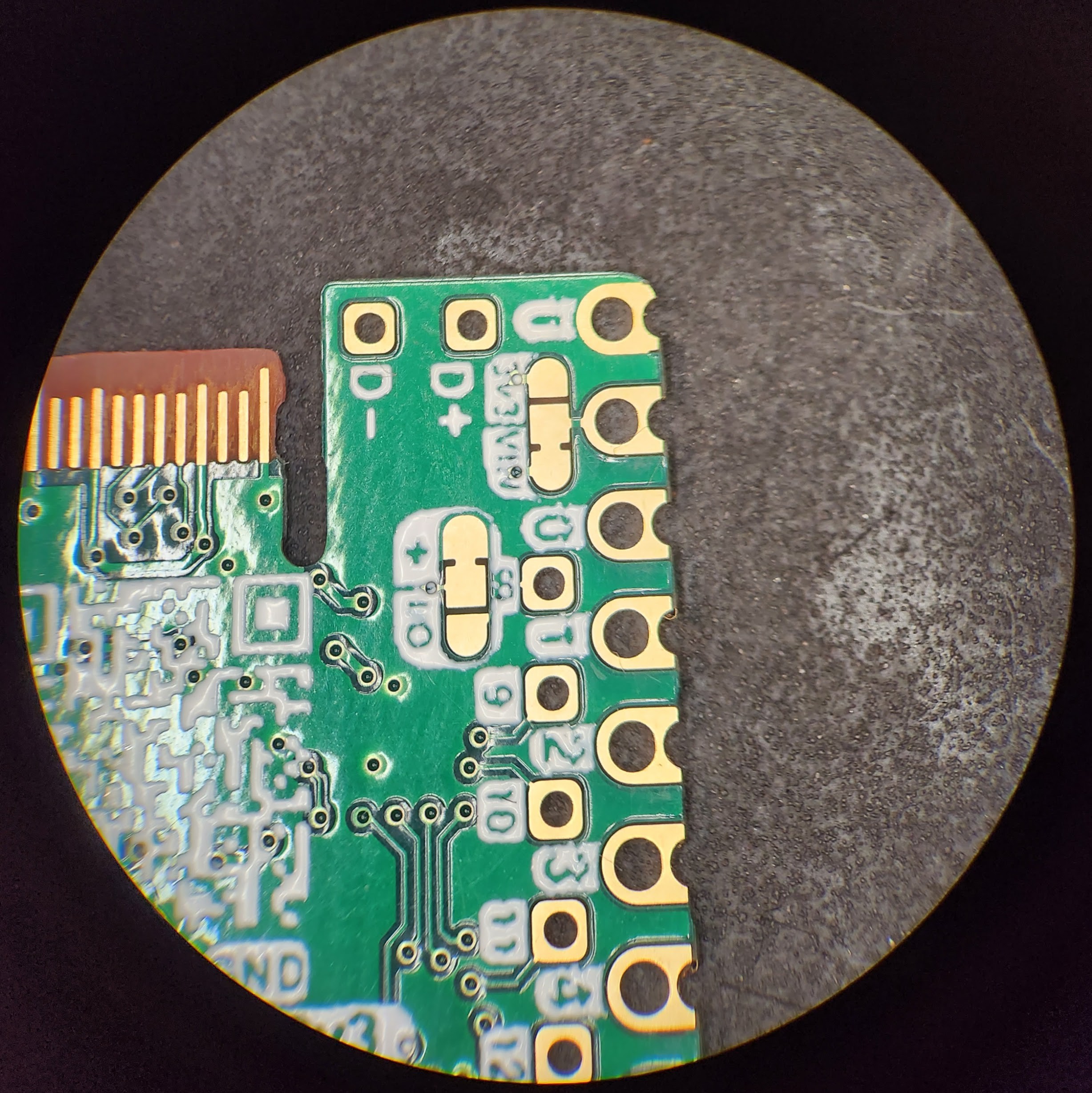
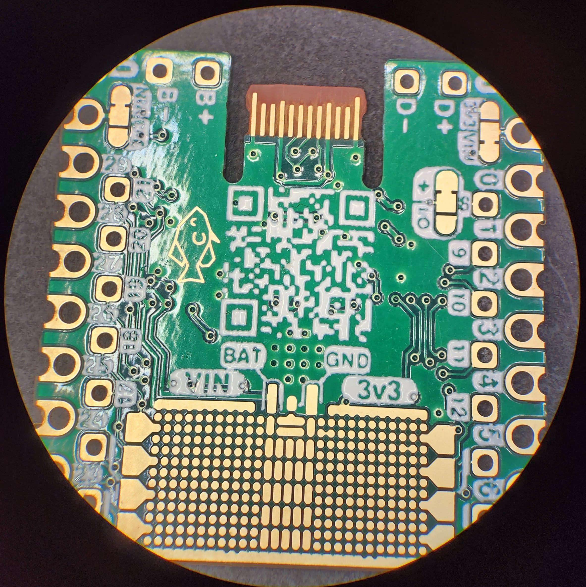
Looking at the labels under a literal microscope, they don't look great. But from a distance they are way better than the silkscreen on Rev 1. Most importantly, it's good enough for my phone to read the QR code on the back! I wasn't sure if that was going to work or not
Even with these tricks though, the poor quality of the JLC silkscreen is pretty apparent. Even worse, the silkscreen seems to be pretty inconsistent. Out of the 20 boards that I ordered, there was pretty wide range of "weights" for the silk screen with either very thick white layers being deposited or very whispy thin layers. I wouldn't really mind the undefined edges, but the inconsistency makes it really hard to account for. I think that in my next inevitable revision I will try PCBWay to see if their silkscreening process is higher resolution... or at the very least more consistent.
And there you have it! Pretty short log for today. In the next one I will finally put one of these things together!
Discussions
Become a Hackaday.io Member
Create an account to leave a comment. Already have an account? Log In.