That's right, Rev. 3 is basically complete and the board is almost ready for public consumption! There are a few different changes that I will get to but first:
A huge thank you to PCBWay for sponsoring this run of pcbs!
While PCBWay sponsored this revision of the CRAPi board, all of the following opinions are my own.
A rep from PCBWay reached out to me after my last post and thanks to his incredible generosity I was able to check out their services. I had never used PCBWay before so I didn't know what to expect, but right off the bat I noticed that the customer service was impeccable. They have a great intake system that let's you correspond with the representative responsible for your boards directly from within the website (as opposed to an email chain). My absolute favorite part of their website was the real time tracking of the PCB production stages. It's really cool to know exactly what stage of the production process your board is in and know when progress is being made.
Really the only negative aspect (which isn't really negative at all) of the proofing process was the final cost/capability assessment. PCBWay takes a very professional approach in their proofing process and if you mis-specify your required manufacturing capabilities (trace width, drill diameter, etc.) they will ensure that those specifications are corrected and that your PCBs match your gerbers as closely as possible. This is in contrast to my experience with JLCPCB, who simply approved my design and sent it off for a best effort approach on their production line, resulting in different via diameters and trace widths than what I specified in my design.
The proofing process resulted in a significant increase in the cost of the boards which was a bit shocking. Given that these boards were sponsored I choose to proceed with their recommended process specifications but in the future I would most likely work more closely with my representative to strike a balance between cost and specifications. It's clear that there is just a higher level of professionalism with PCBWay!
Once that boards were done they arrived via DHL in just a few days. Incredible! I think they turned out very nicely.
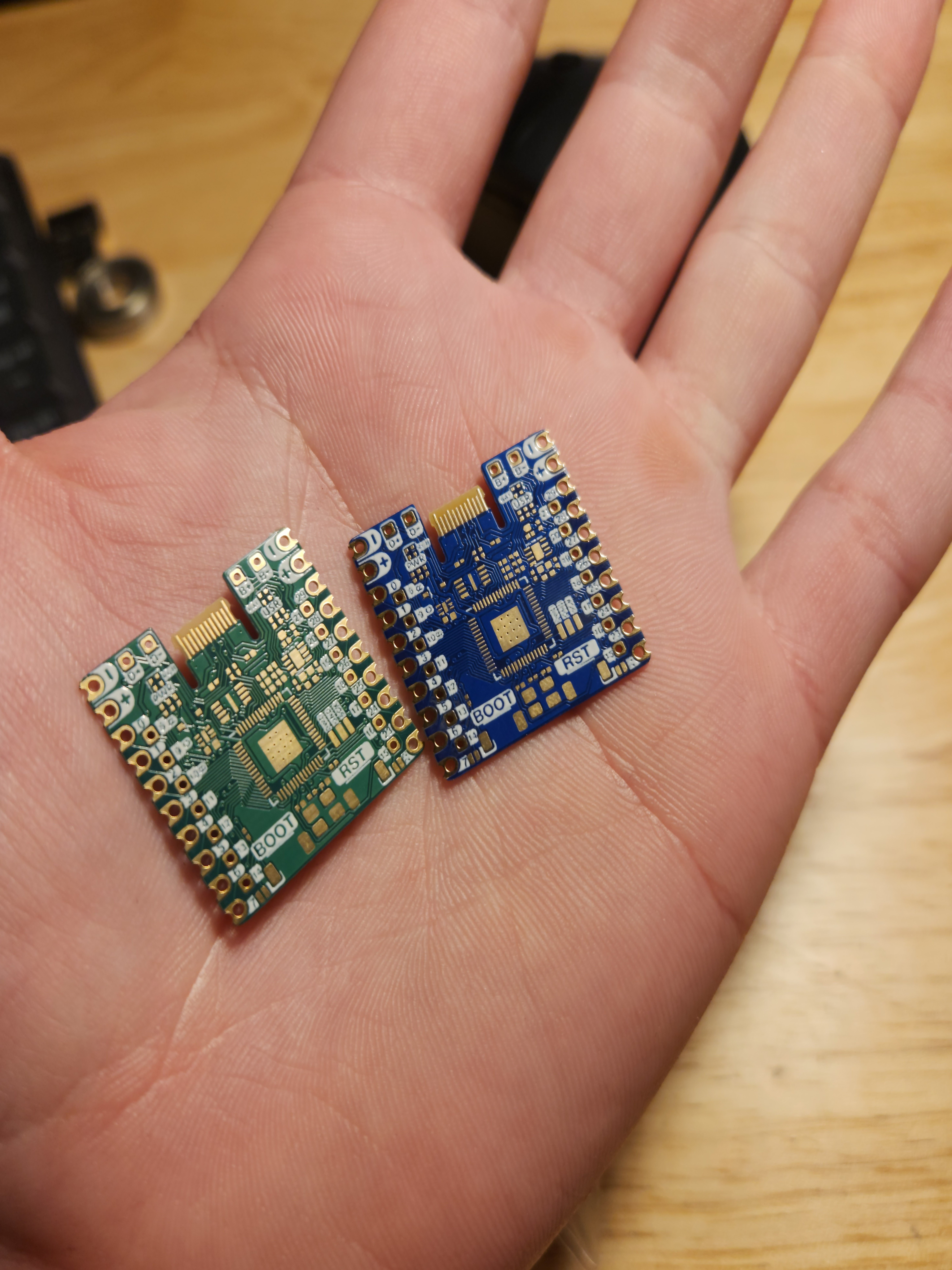
This time around I was curious about how the thickness of the PCB would effect the retention force of the USB connector. The green boards are the 0.6 mm that I have used for the previous revisions and the blue board is 0.8 mm. The USB-C specification is 0.7 mm. The blue boards were almost impossible to disconnect accidentally. The force required to unplug it was almost too high. It also appears that the contacts on the blue board slowly get mushed down after repeated connections. I need to do some more repetitive testing before I decide on a final thickness and weight the costs and benefits of the thicker board.
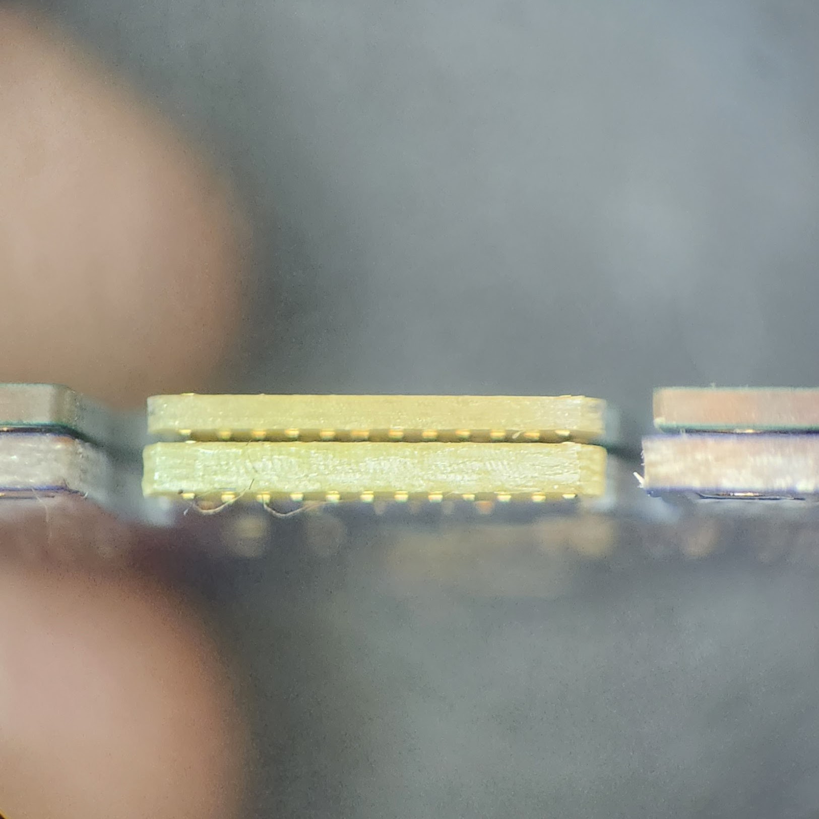
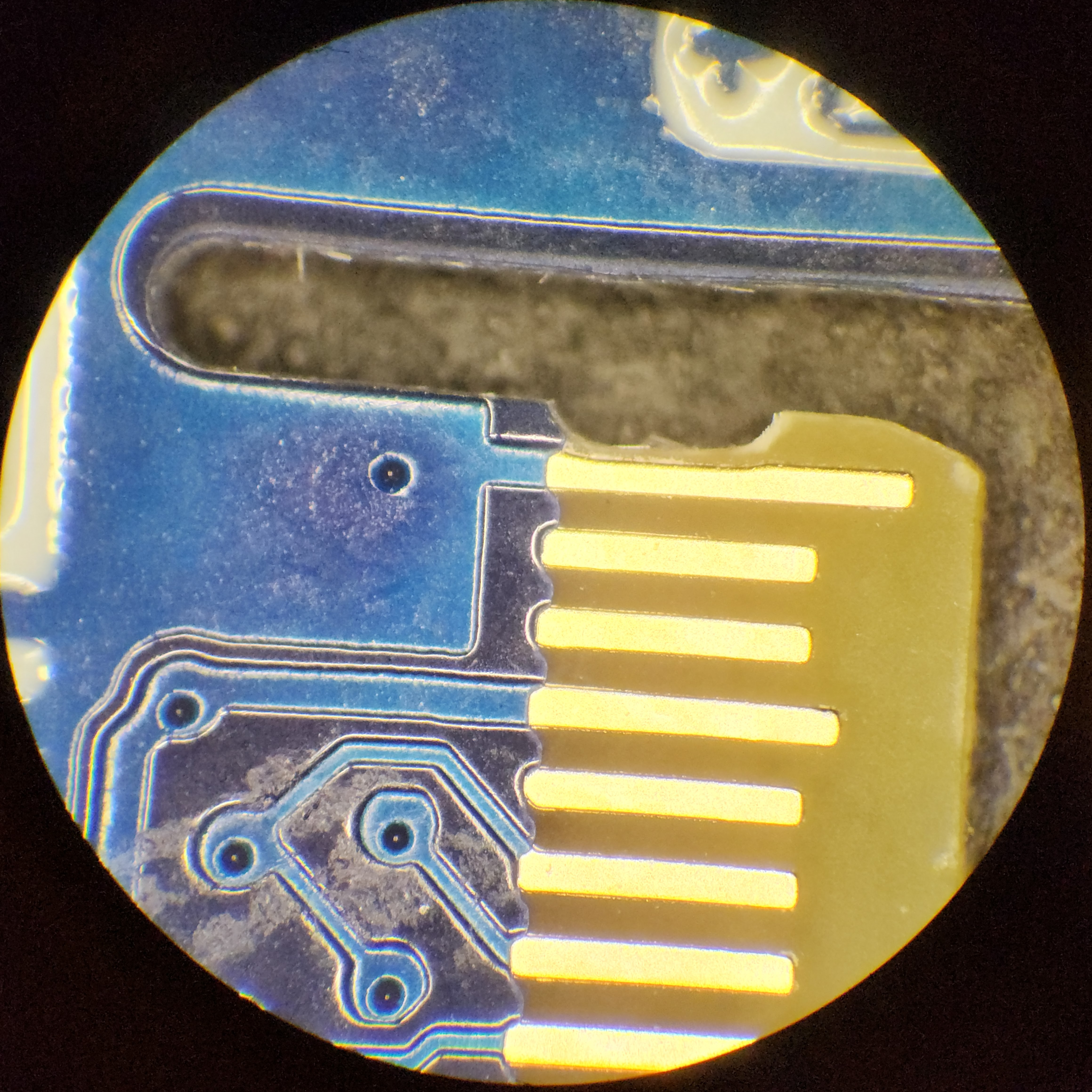
PCBWay also did a superb job routing the small detents into the side of the USB-C connector. Previous revisions that used the JLC boards were far less crisp and the increase in quality is evident in the improved retention force of even the 0.6 mm thickness.
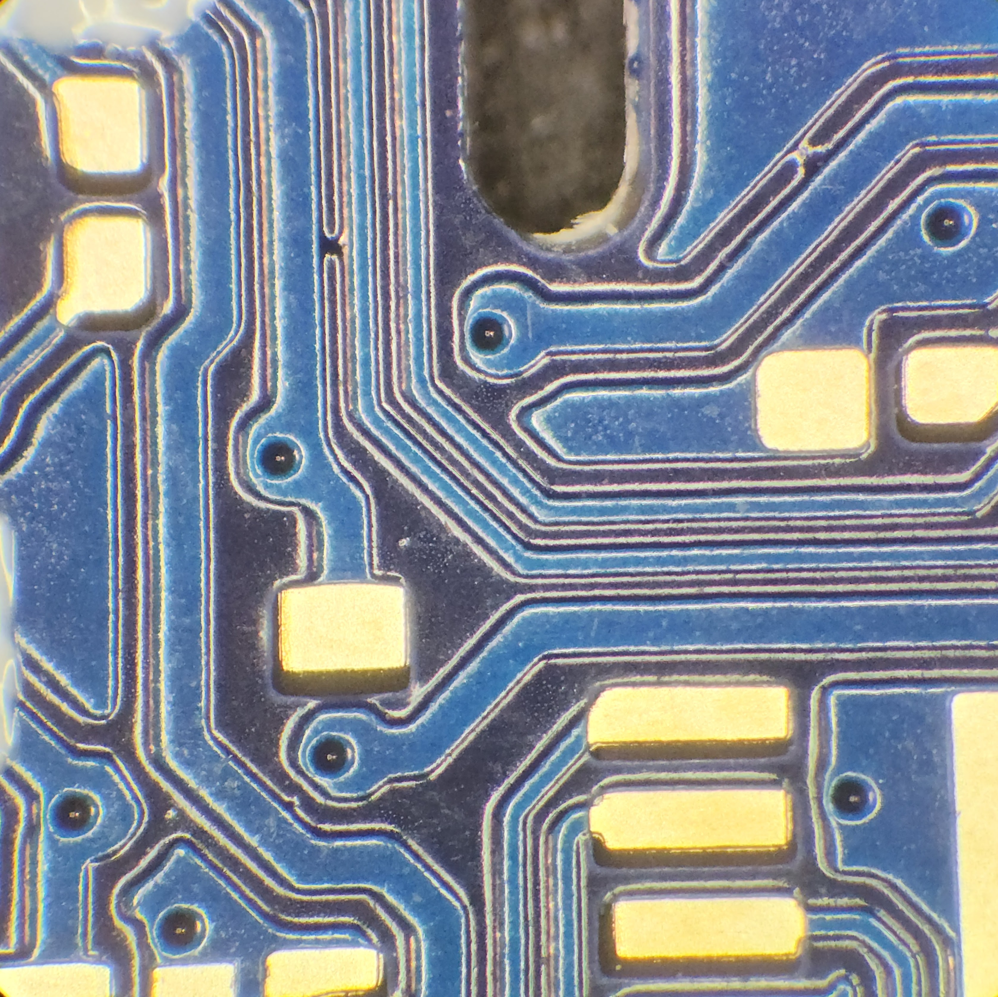
Really the only criticism of their build quality was a slight mismatch on the registration of the vias. The vias uniformly off-center from their desired locations across the entire PCB. It's quite possible there could have been an issue with my gerbers, or that I am simply pushing the limits of their production capability. Nevertheless, they were all consistently covered with soldermask and this slight registration mismatch didn't cause any problems.
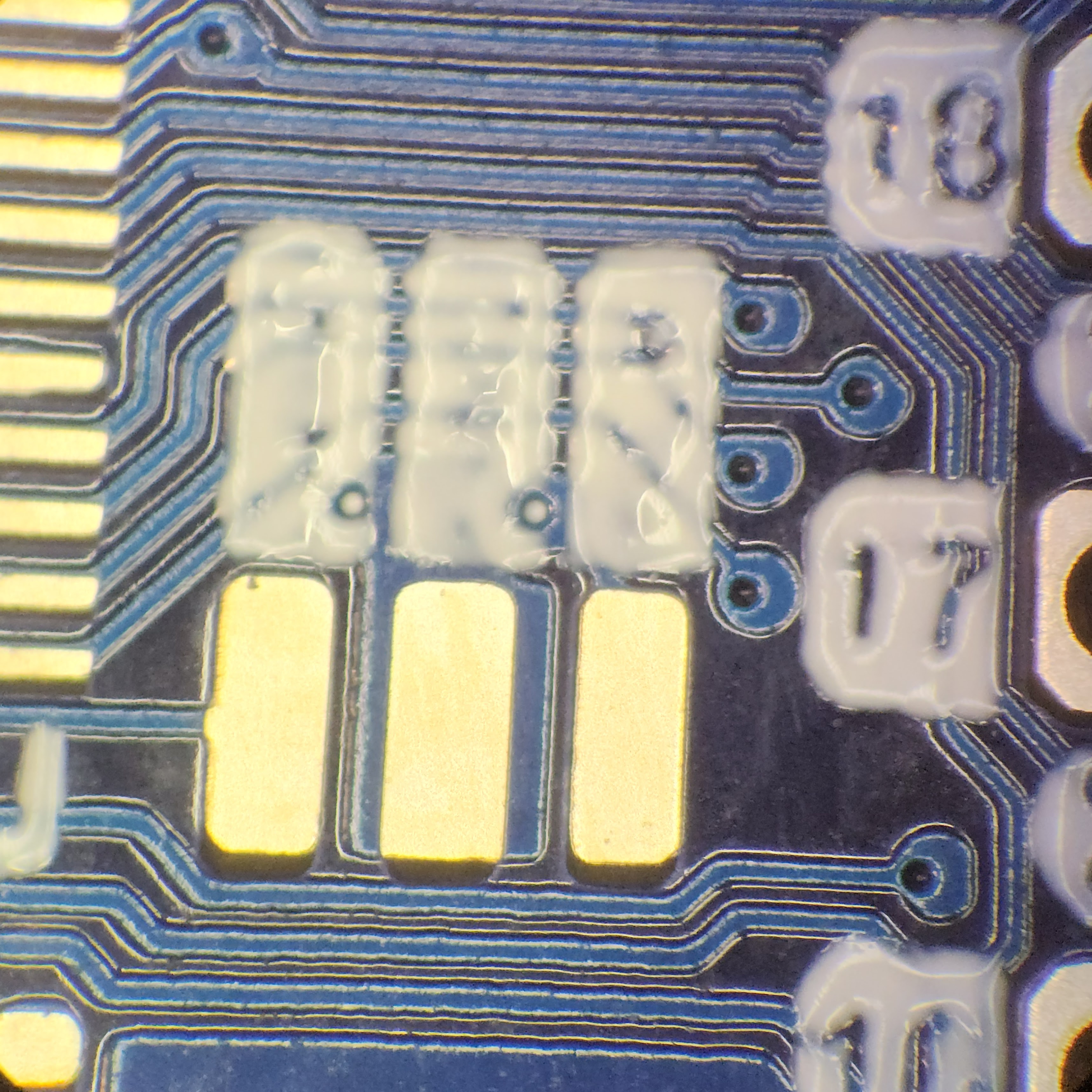
I was curious about the quality of PCBWay's silkscreen. I didn't have expectations because I am working at the limit of the typical liquid photo imaging (LPI) silkscreening process. Next time I order PCBs I am going to make sure to select the direct legend printing option so that all my labels can finally be read. That option is a flat 80 dollars so unless I am ordering a bunch of boards it hasn't been worth it, yet. The legends below are supposed to be labeling the debug header...
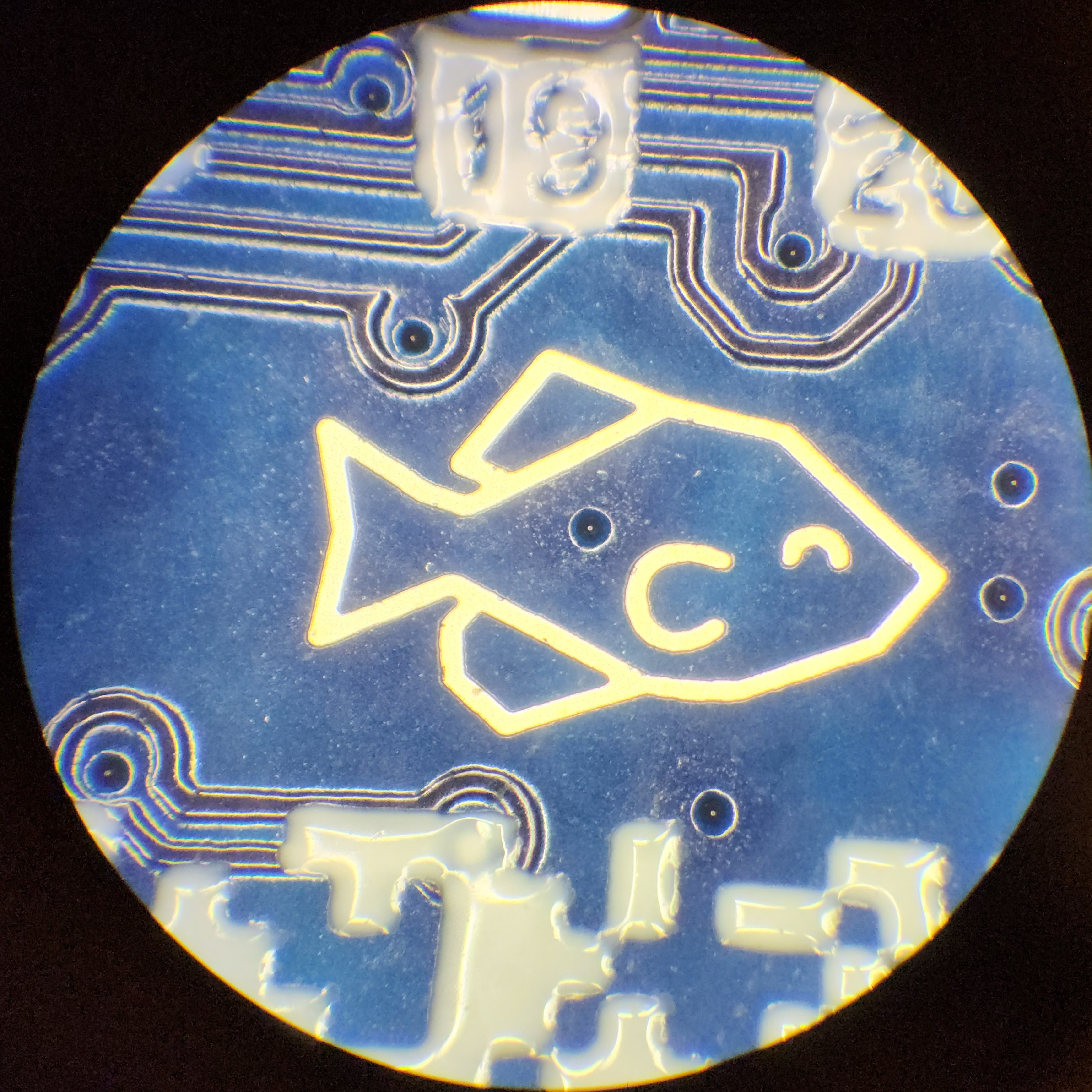
The solder mask capability on the other hand is impeccable, as expected. Look at that happy little crappy!
So overall I am very happy with the quality of the boards that I received and of course I would like to extend a huge thank you to PCBWay, again. I will definitely be ordering from them in the future and I encourage you to check them out. I plan on selling these boards so I am also very interested to trying out their PCB Assembly service.
What changed and where are we now?
There were a few major changes that came along with Rev. 3:
- A better Protogrid
- 20 mil spacing is much more usable and targets SOIC-8 packages
- Larger pads that wont fall off and are hand solderable
- A Qwiic connector foot print
![]()
- Raspberry Pi Pico compatible debugging foot print
- I managed to jam in the same footprint that the Pico uses for the debugging port, which makes this board compatiable with the Raspberry Pi Debug Probe connectors.
- An improvement of the two tiny little testpoints I had before.
![]()
- More efficient power switching / battery charger
- The addition of a P-FET in an ideal-diode-like configuration means we are dropping a fraction of the voltage we were with the previous schottky-based approach.
I think the next spin of the boards should be ready for public consumption. I did have one major mistake because I forgot to re-enable some DRC settings and accidently shorted 3.3V to ground. Some quick work with a razor took care of that though. At least it's an easy fix!
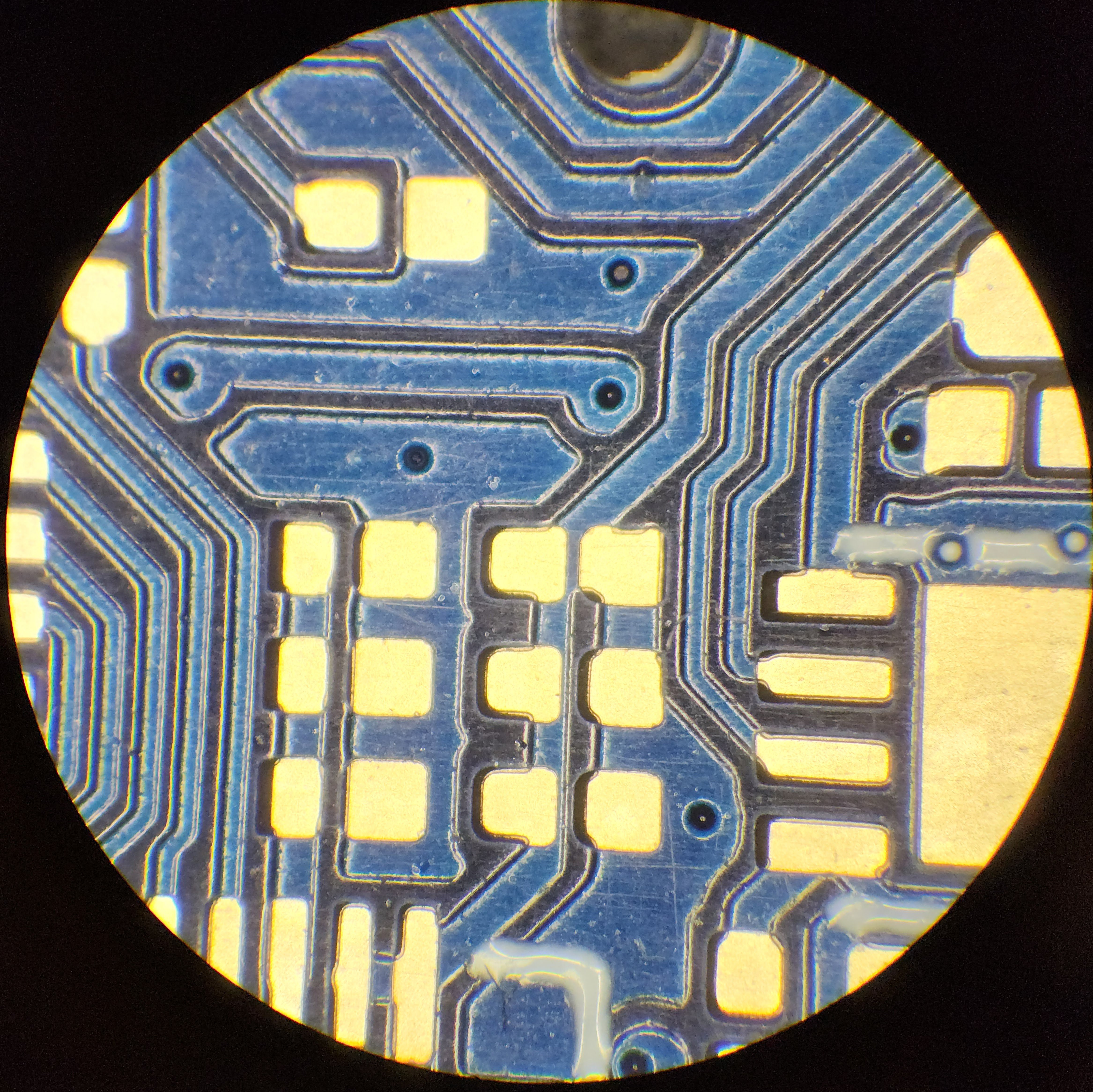
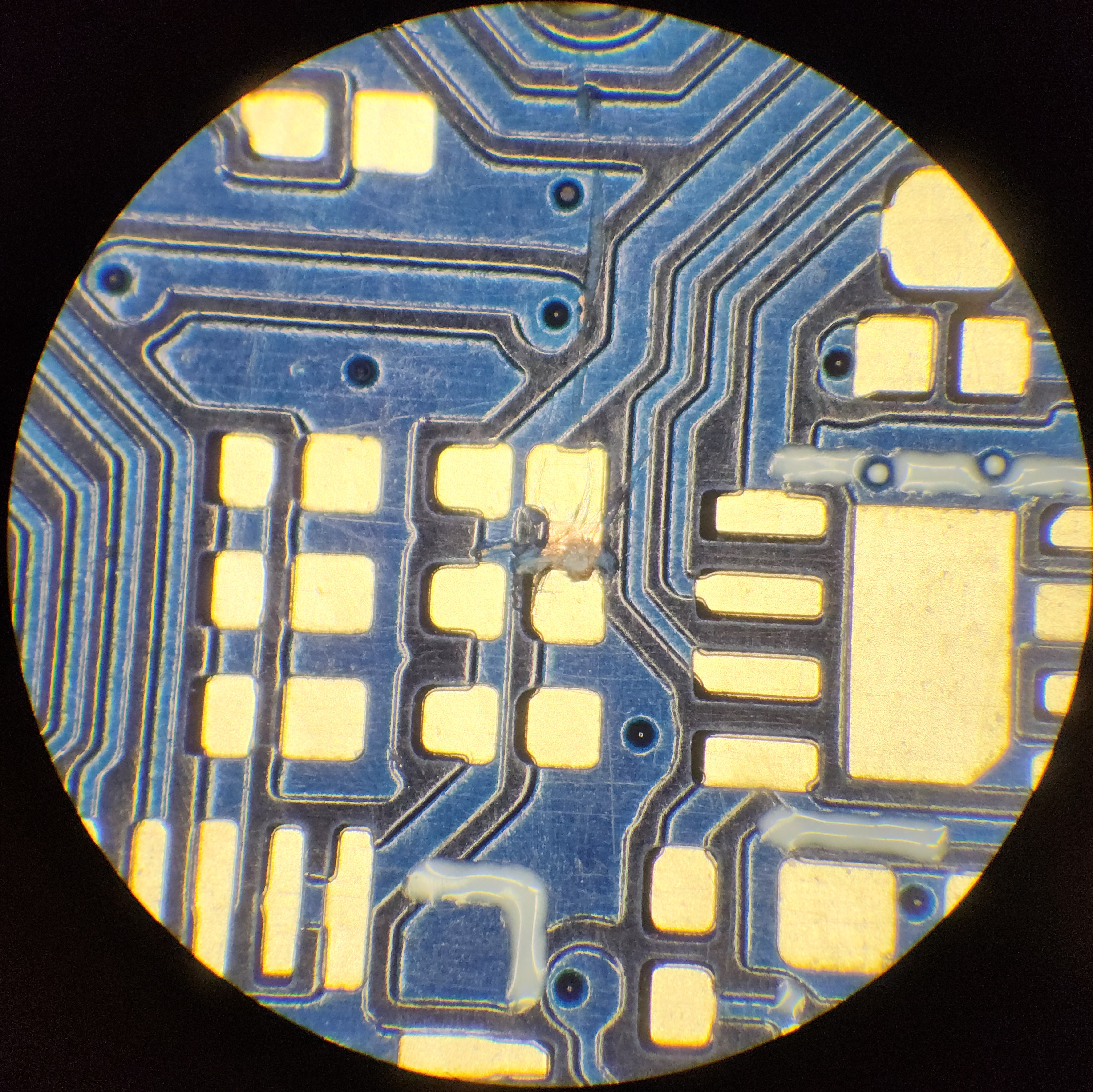
As this project enters its second year I want to thank everyone who has been following along. Sometimes it feels like we are asymtotically approaching completeness but I think the end is in sight!
 Chris
Chris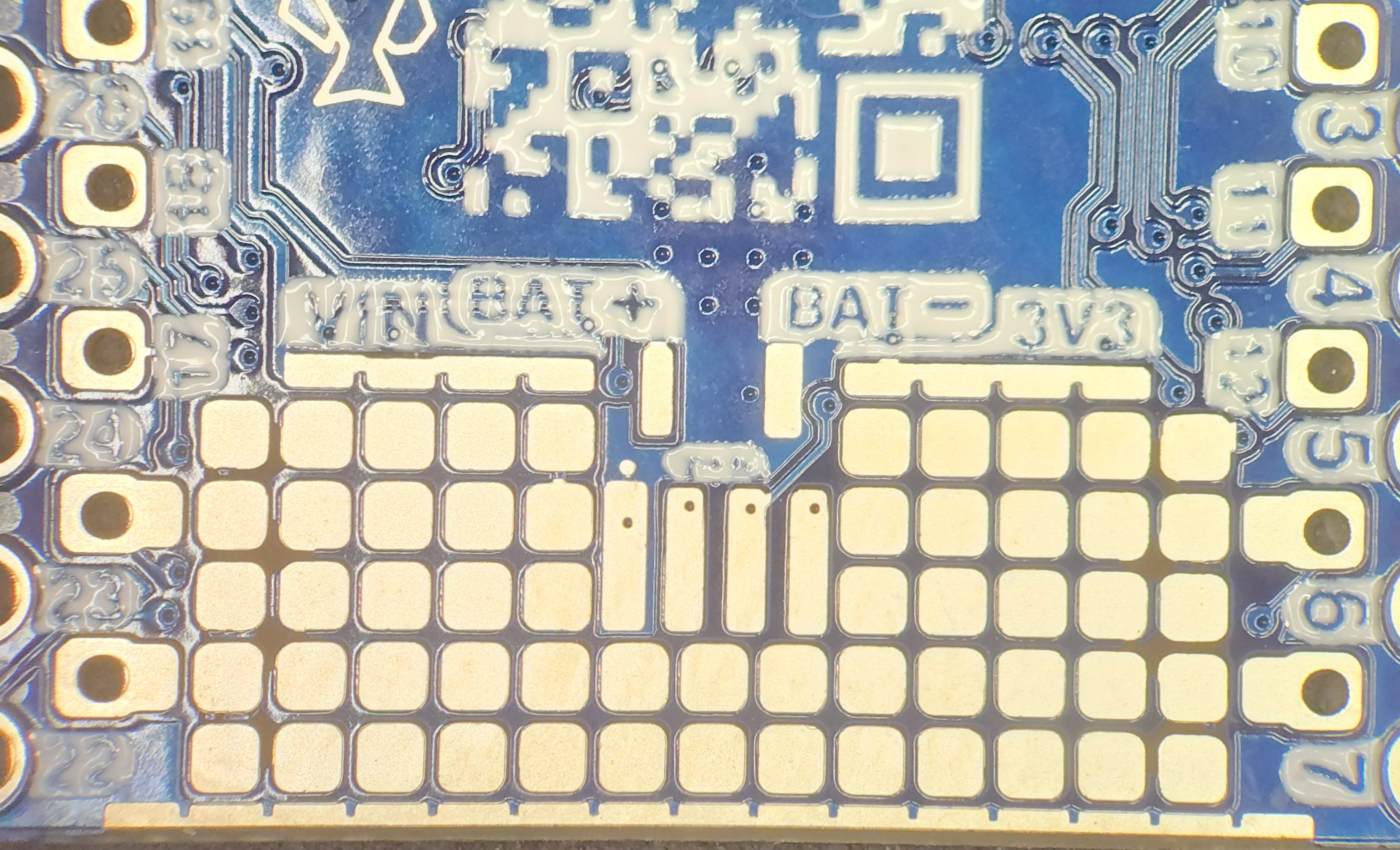

Discussions
Become a Hackaday.io Member
Create an account to leave a comment. Already have an account? Log In.
Very cool. However, no matter how much you improve it, it's still going to be a CRAPi PCB. ;)
Are you sure? yes | no
that's the idea!
Are you sure? yes | no