 c00
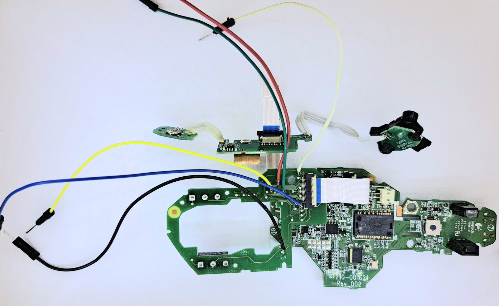
c00Chip package type is WLCSP with diagonal pin pitch 0.4mm. Luckily boards don't appear to have more than 2 layers, and size of vias suggests that all pins are fanned out to the sides.
After careful examination under microscope I've identified following pinout of ribbon cable:
- GND
- ?
- "Hidden" button
- ?
- SCK
- SDO
- CSB
- SDI
- ?
- VDD_IO 2V - voltage is dropped to 1.6V for VDD with local regulator
- ?
- ?
There are no points on the little pcb available where wires could be soldered without removing connector. Luckily all connector pins have a test points on the next board that ribbon cable connects to.
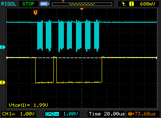
To confirm pin assignment I tested them with oscilloscope. SCK and CSB pins checked out, but there is no activity on SDI, and SDO.
Discussions
Become a Hackaday.io Member
Create an account to leave a comment. Already have an account? Log In.