 Keith
KeithOne can add slow mode hardware to a ZX80, but I decided to buy a board with this designed in already.
https://revspace.nl/Buiding_up_and_testing_the_ZX81%2B38_revision_1,9
https://github.com/mahjongg2/ZX81plus38
2023-08-19
I bought these boards on eBay.
The logic board has some nice features. The bus signals are available on a holes for a header, allowing the dreaded RAM-pack wobble to be avoided. The board can take up to 32K RAM, so you don't even need an external RAM pack.
Power is from a USB-B socket. I'll have to check the electric current budget.
On the down side, the clock is a crystal-and-inverter which mean I can't change frequencies by swapping an oscillator can. I think that can be hacked!
The on-board SLOW-mode generator will need hacking to run with a 14.7456 MHz clock. I'll design something that can be easily switched between two frequencies.
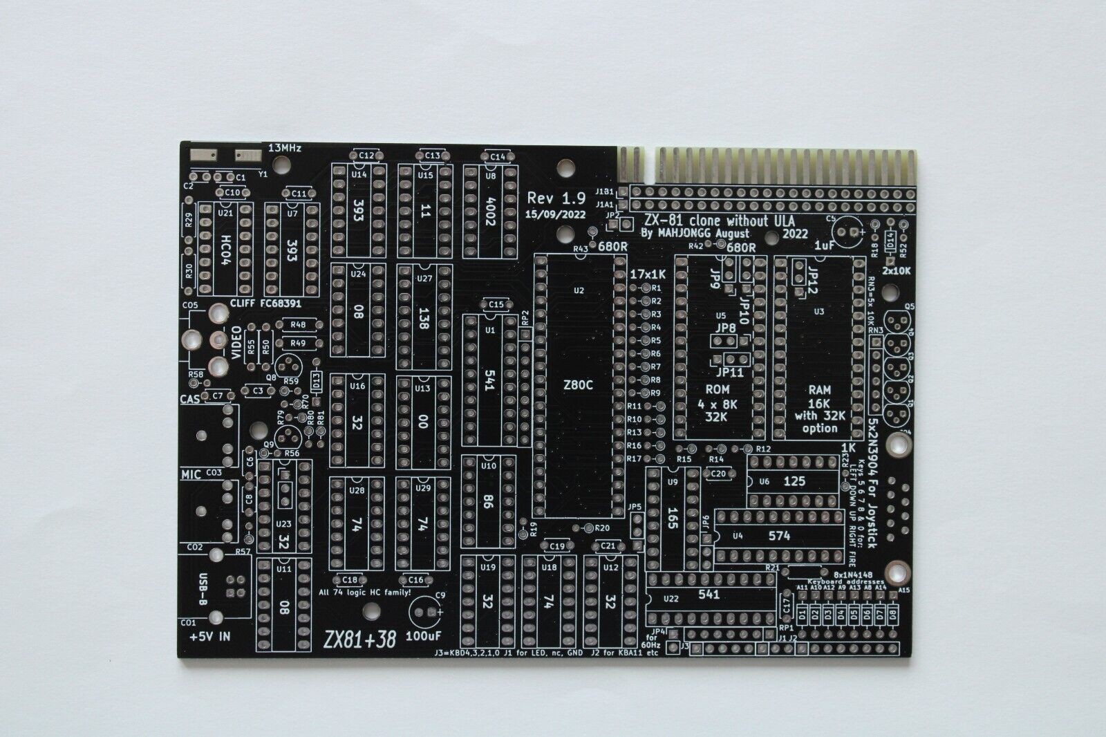
The keyboard is on a separate PCB, so no mechanical stress is transmitted to the motherboard. It has the key letters but not the associated keywords.

The boards are due in about a week, so I shall get hunting for components.
2023-08-21
Printed out the circuit diagram and parts list. I have:
- Z80 CPU
- ROM
- RAM
- HC165 shift register
- HC74 D-type latches
- HC04 inverters
- HC138 one-of-eight decoders
- ACT86 xor-gates
- ACT574 eight-bit edge-triggered latch
What I don't have:
- HC541 (but I could use some ACT245 with a bit of hacking)
- HC08
- HC32
- HC125
- HC393
- HC4002
I could use some PAL chips to mop up the random logic. I have plenty and they are easy to modify.
2023-08-23
Boards arrived. I have soldered the key switches to the keyboard.
The motherboard is very packed.
2023-08-25
I fitted 0603 surface mount resistors where there are vertical through-hole resistors.
The ACT574 and HC165 chip are now soldered to the board.
2023-08-31
I have no HC541 chips but plenty of HC245 chips. So I took two HC245 chips and bent pin 1 under the chip and wired it to VCC. I then fitted it to the HC541 sites.
2023-09-27
Fitted SIL sockets for keyboard.
2025-04-25
- Found HC08 and HC32 chips
2025-05-18
I decided to fit all the chips that were not completely used in the HSYNC and PORCH timing. This is basically all of them except U15 (a 74HC11) and U8 (a 74HC4002).
I plan to replace these with a GAL16V8, with more sophisticated timing, for both normal and square pixels.
The signals q7 down to q0 are on U14.
The asynchronous reset is on U15 pin 8.
The output signals PORCH and HSYNC are on pins 1 and 13 of U8 respectively.
So not a huge wiring job. Some pins can be piggybacked on the 74HCT393.
2025-05-29
Shopping around for the last few bits for this project. I wondered why the Mouser 13 MHz crystal in the BOM did not appear in my search for crystals, and I spotted that the footprint is completely incompatible with the PCB. It has leads 2.5 mm apart, while the PCB has holes 4.88 mm apart. The PCB uses an HC49 footprint, not an HC46 footprint. So, the most suitable part seems to be IQD part LFXTAL031646B which is Mouser part 449-LFXTAL031646BULK. Also note that wire-ended crystals will need some insulation from the SMD footprint pads, otherwise the metal body will short-circuit them. See Mouser part 520-700-TFL-9001.
2025-11-11
Fitted R12,14,15, RP1, RP2, X1, original 2364 ROM.
2025-11-12
Applied 5V through USB cable, but failed to boot up. The current drain was exactly 100mA, which makes me wonder if it wanted more but was being limited to the USB peripheral limit. In another USB socket labelled 5V 2.1 A, it was 4.886 volts measured at the power input socket, 4.872 at ROM pin 24.
5V pins connected to each chip.
Sigh, I'm going to have to get out the scope and do a lot of hard work. :-(
2025-11-17
Identified the problem. I was using an original 2364 ROM, which has socket pin 20 (2364 pin 18) = A11, and socket pin 22 (2364 pin 20) = /CE. The latter is permanently wired to nROMCS. The bug in the design is that the signal from socket pin 20 was also named nROMCS. Which means pins 20 and 22 are permanently wired together. The 2364 ROM cannot be used. Had the track from pin 20 been named something sensible like P20, then link JP11 might have allowed pin 20 to be nROMCS or A11. It is currently redundant, because the default position duplicates what the PCB tracks already do, and the other position will simply join nROMCS to A11, causing a short-circuit.
A similar mistake exists for socket pin 23, the track is named A11 which means it is always wired to A11, so JP8 is redundant in the default position and shorts A11 to A12 in the non-default position.
The same goes for JP9.
Only JP10 gets it right, by naming the track from pin 27 as P27.
These errors are in circuit version 1.9 (the board I have) and 1.10 (the latest version).
The work-around is to use a ROM device that has pins 20, 23, 26 as /CE, A11, A13 respectively.
2025-12-28
A quick look through my programmable parts box shows some 32-pin Flash ROMs and a pair of 28C64 EEPROMs. The latter seem suitable for a quick test. Pin 27 linked to VCC. Still not working.
2025-12-29
Found a dry joint at R42 and the connection to the ROM. Fixed, and it now boots to the K prompt... sometimes. I put the latter down to the simple RC reset circuit of R52/C5. This gives around 10 ms reset pulse, but the /RESET pin really ought to be driven by a faster-rising pulse from a decent reset circuit.
Looking at the video on screen, the black edges are immediately followed by a bright white shadow. This overshoot is caused by impedance mismatch. This is typical of home computer designs of the 1980s, cobbling video drive from shoddy one-transistor circuits. The video output impedance of this circuit is 100R when low and 50R when high. It ought to be 75R at either level.

You can also see a faint dark vertical line on the left of the screen, another result of the poor video circuit.
So for now, most of the circuitry is working. The reset and analogue video circuitry could be improved a bit.
2026-01-01
The video output circuit looks weird. I'm mostly digital but I can do a bit of analogue, and I can see that the output impedance is going to be two 100R in parallel = 50R. Also, when the sync pulse is low, there will be no base-emitter current and the impedance will be 100R.
The output impedance is meant to be 75R. Other designs tend to have a resistor from emitter to ground, then a resistor from emitter to video output (75R less the transistor's emitter output impedance which is about 12R6, i.e. 62R4, or 62R as nearest E24 value).
The emitter impedance is only low if it is carrying some base-emitter current. If that is cut off completely, impedance goes high and we don't want that. This is avoided by having the sync level non-zero but low enough to work, say 0.1 volts.
If the sync/black/white voltages are 0.1. 0.4 and 1.1 at the monitor, they need to be twice that (0.2, 0.8 and 2.2 volts) at the emitter, and then 0.7 Vbe above that at the base (0.9, 1.5 and 2.9 volts). I'm not sure how to calculate the resistor network required for two 0/5 volt logic inputs. But it is easier if both are open-collector signals. I thought of using a 74HC4052 to select voltages, but the switching time is 28 ns, compared with around 4ns for a 2N2222 transistor.
Discussions
Become a Hackaday.io Member
Create an account to leave a comment. Already have an account? Log In.