 CentyLab
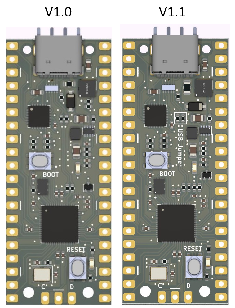
Learning from the previous design, I have made some changes to the layout while keeping the schematic the same. Here are some main changes:
- Highlight 0-ohm jumper resistor: To use the USB 2.0 header, remove these 2 jumpers.
- Highlight GND ports on the top layer
- Thermal relief for the USB header: Easier to solder and desolder
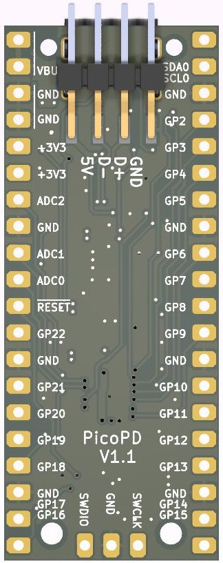
The next October 25th,2023 batch will be V1.1. You can make your own using the provided Gerber, else you can support me through Tindie PicoPD.
Discussions
Become a Hackaday.io Member
Create an account to leave a comment. Already have an account? Log In.