MatNieuw
About this project
In 1838-1858, Charles Babbage designed a programmable (punch card) digital mechanical computer, the analytical engine, with conditional branching and loops. It was never built, as it was too difficult.
From 1938 to 1941, Konrad Zuse built a programmable (35 mm film) digital electromechanical computer (relays). It worked (22 bits floating point), but had very limited capabilities (no jumps, no tests, no subroutines).
After seeing a replica of the Zuse Z3 in Berlin, I thought: Babbage had the idea but not the technology, Zuse had the technology but not the ideas. What if Zuse had had the ideas?
This project is about designing circuits that could have been made with the technology available at the time (i.e., no semiconductors). Whether I will actually build a computer with it is undecided yet.
General technology
These circuits assume 3 logic states: 0 (GND), 1 (=relay activation voltage), Z (high impedance). The 0 and 1 should be able to source and sink the current of a number of relays (limited by relay contact current). Relay settling time is represented by the letter T (e.g. 5 ms, likely slower for pre-1940 relays). Pre-1940 there were no reliable diodes, relay coils should have something to damp large voltage spikes. A small neon bulb over the coil limits the spike for my relays to about 125V, a R of coil resistance and C of 10 nF in series over the coil limited it to about 225 V. Measurement with an oscilloscope shows neither method slows relay settling time (a diode does). This damper circuit is not shown in the circuits.
All relays are 2 form C (DPDT), because they are easy to get now. Pre-1940 4 form C (4PDT) would be available, and save quite a few relays in certain circuits, like the DRAM/ROM address decoders.
Tools used
- Circuit drawings: KiCad, can do PCB drawings too (but cannot simulate relays).
- Simulations: circuitjs. Not all circuits might have simulation files. circuitjs1 offline use: https://www.falstad.com/circuit/offline/
circuitjs1 online use https://www.falstad.com/circuit/
- Timing diagrams: wavedrom-rs https://github.com/coastalwhite/wavedrom-rs/releases
Clock generator
Choose R1 so that the relay reliable engages.
R2 is ideally such, that the parallel resistance of the relay coil and R2 equal R1. In the example, 1500 parallel with 700 gives 477 ohm.
R2 determines duty cycle (within limits), I got 75+85 ms per cycle. Different relays will need different component values.
C1 determines frequency, in my test I selected for 6 Hz. Lower C1 values give higher frequencies, but the relay switch time becomes a larger part of the total cycle time.
If the clock generator drives only a single DPDT relay, that relay can be wired to provide both clock and inverse clock, with some small dead time between the two due to relay switching time.
With another relay one could at selected times add Cs parallel, to lower frequency, when a slower clock is desired e.g. for a slower circuit. Such a C should always be connected to GND at the minus side, and permanently fed at the plus side via a high resistance value (say, 1 M Ohm) from a voltage equal to the lowest voltage on the relay, to prevent wrong pulses when it is switched parallel to the existing C.
Latch with clear
This 2 bit latch uses the fact that the hold current of a mechanical relay is lower than the activation current. VDC is the relay voltage.
Choose R1 and R2 so that the relays reliably holds. In my tests, with 24V/700ohm relays, 1k2 ohm gave the minimum hold voltage according to the datasheet, but my relays held fine with 1k8 too. It saves considerable energy too, when in hold mode.
If the "write" relay is activated, input data (here D0 and D1) is connected to the associated latch relay. If the input is VDC, a latch relay will be activated if it was not, otherwise it stays activated. Once activated, it stays activated if K1 is de-activated because of the R. During the latch relay activate time there will be a current from VDC to GND which is higher than the normal relay current (because of the R), but it lasts only a short time until the normally closed contact starts moving.
If the input is GND, and the write is activated, a latch relay will get 0 volts across it and is de-activated.
This circuit can be expanded to as many bits as required. The latch has both normal and inverted outputs, which is very useful in some cases.
Propagation time: input-to-output: 2 T, clear-to-output 2 T.
D-flipflop with clear
This one bit D-flipflop uses two latch circuits in series, separated by a clocked relay. A latch works fine for just storage, but if the output might need feedback to the input, a separation in time is needed.
Propagation time: input-to-output: 4 T, clear-to-output 2 T.
For the latch details, see the latch circuit.
Ripple program counter with parallel load
Per bit, a D-flipflop in divided-by-two mode, which each flipflop clocked by the output of the previous bit. With an extra relay to allow setting the counter to a selected value (when a jump in the code occurs). Uses 8 relays per 2 bits.
Propagation time input-to-stable-output: 2 + 2 * number of bits T.
For D-flipflop details, see the D-flipflop circuit.
If you run the simulation in counting mode with circuitjs, you can clearly see the propagation delays. The simulation has 4 bits, with LED added for clarity, and allows setting load values.
Dynamic RAM
This extendable 2x2 bit DRAM memory uses capacitors as storage elements, and one tube per bit line to translate capacitor voltage to relay voltage, and "tops up" the capacitor voltage at each refresh. The circuit can be extended as desired, say 1024x32 bits.
Write operation timing 3 T: set address 1 T, enable write relay 1 T, release write relay 1 T.
Read operation timing 4 T: set address 1 T, enable refresh relay 1 T, enable read relay 1 T, disable read relay 1 T.
Refresh timing: 6 T: switch address bus to the refresh counter and set address 2 T, enable refresh relay 1 T, wait at least 1 T, disable refresh relay 1 T, remove refresh counter from address bus 1 T .
Before 1940, there were multiple power output tubes likely suitable, e.g. the AL3 (from 1935). The "leak" quality of the C's of that time I don't known.
The circuit was tested with one triode of a PCC84 (equivalent of ECC84) tube with a 4 x 1 bit DRAM.
Refresh times can be very long, testing so far with 1970's Cs after 14 hours there was still enough charge. With an old 250 nF C however, it was just 4 minutes. So C's would have to be selected for low leak.
Of course, additional relay circuitry is needed for a refresh counter, and at refresh times do a non-data read with the address coming from the refresh counter.
Fast adder
Joe Allen's fast adder circuit, see picture for details.
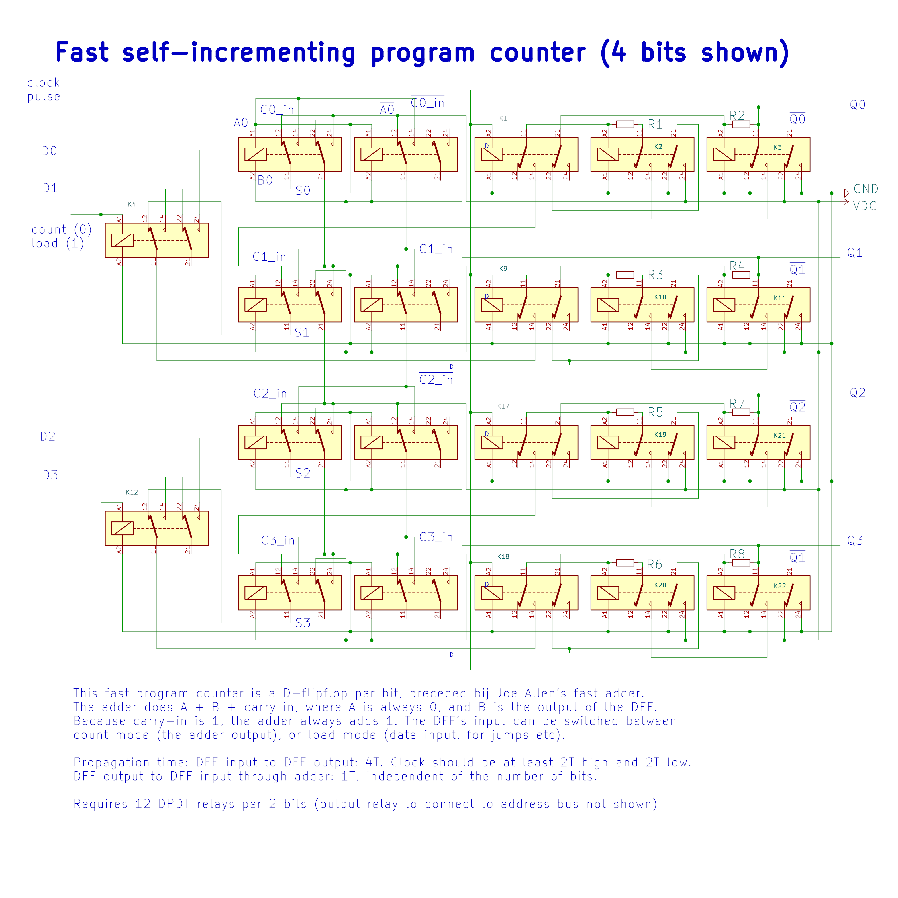
Fast program counter with parallel load
Per bit, a D-flipflop preceded by an "add one" fast adder.. With an extra relay to allow setting the counter to a selected value (when a jump in the code occurs). Uses 11 relays per 2 bits.
Propagation time input-to-stable-output: 2 + 2 T, then 1 T for the output of the fast adder is updated.
For D-flipflop details, see the D-flipflop circuit.
If you run the simulation in counting mode with circuitjs, you can clearly see the much faster propagation delays compared to the ripple program counter (at the expense of 3 extra relays per 2 bits). The simulation has 4 bits, with LED added for clarity, and allows setting load values.
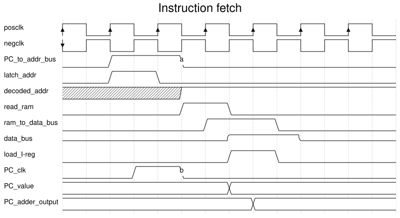
DRAM read access timing diagram
Timing diagram for fetching an instruction, using the fast program counter circuit and DRAM. The DRAM address decoder has a latch added before it, so the DRAM address stays stable until a new address is used. This reduces wear on the address decoder relays.
The clock is 1T high and 1T low.
9 T after enabling the PC, the data bus is free for other use. 4 T after enabling the PC, the address bus is free, but cannot be used for DRAM until 7 T .
The timing for reading other data from memory is the same, the source of the address and destination of the data would be different. A new read can be done every 9T. Writes (not shown) are faster, 6T. Filling a memory area with a value (e.g. a 1, to test memory) is even faster, probably 4T, because the address can stay on the address bus, and only the write latch has to be disabled while the address changes to the next value.
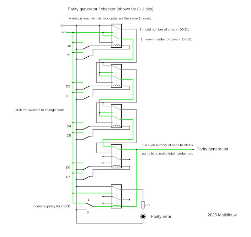
Parity generation/check
Simple parity generator/checker, using 1 relay per 2 bits, plus 1 for the check.
Propagation time 1 T. Simulation file for circuitjs provided.
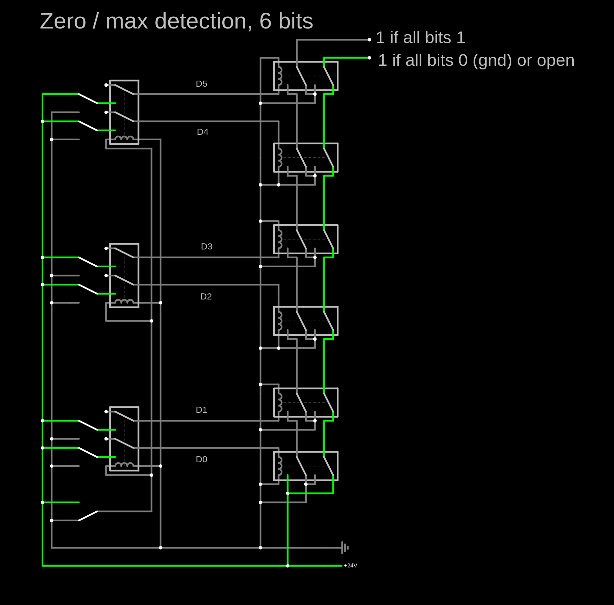
Zero and maximum detector
This circuits uses one DPDT relay per bit to detect both an all-zero and and all-one value.
Propagation time 1 T. Simulation file for circuitjs provided.
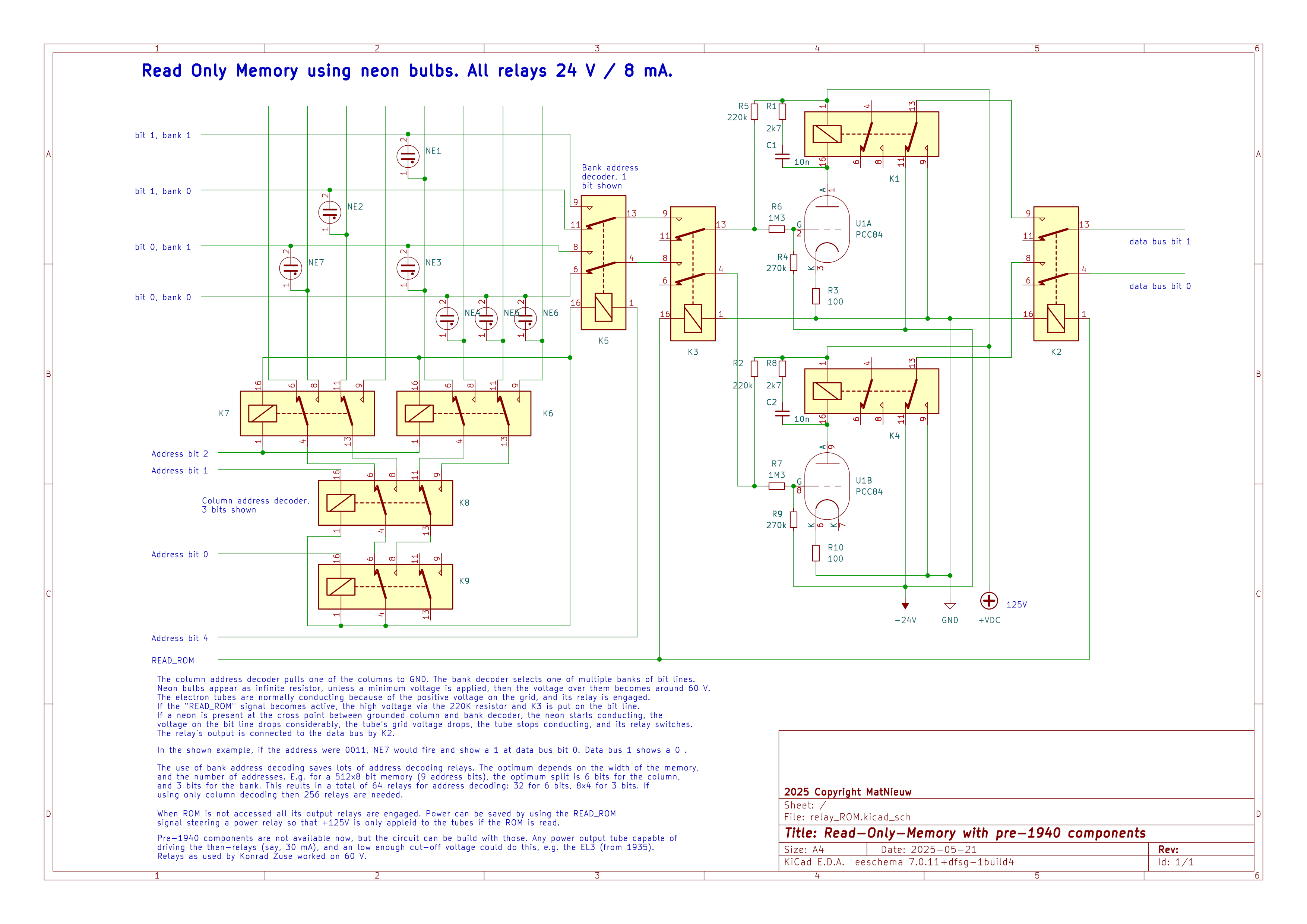
Read-Only-Memory
Based on a column/row matrix of neon bulbs. Where there is a neon, there will be a 1 at the output if the ROM is read. This memory can be build using pre-1940 components (f you can get them), using larger-current relays and tubes that can drive them (see DRAM description).
Access time 2 T from activation of the read signal until the data is on the data bus.
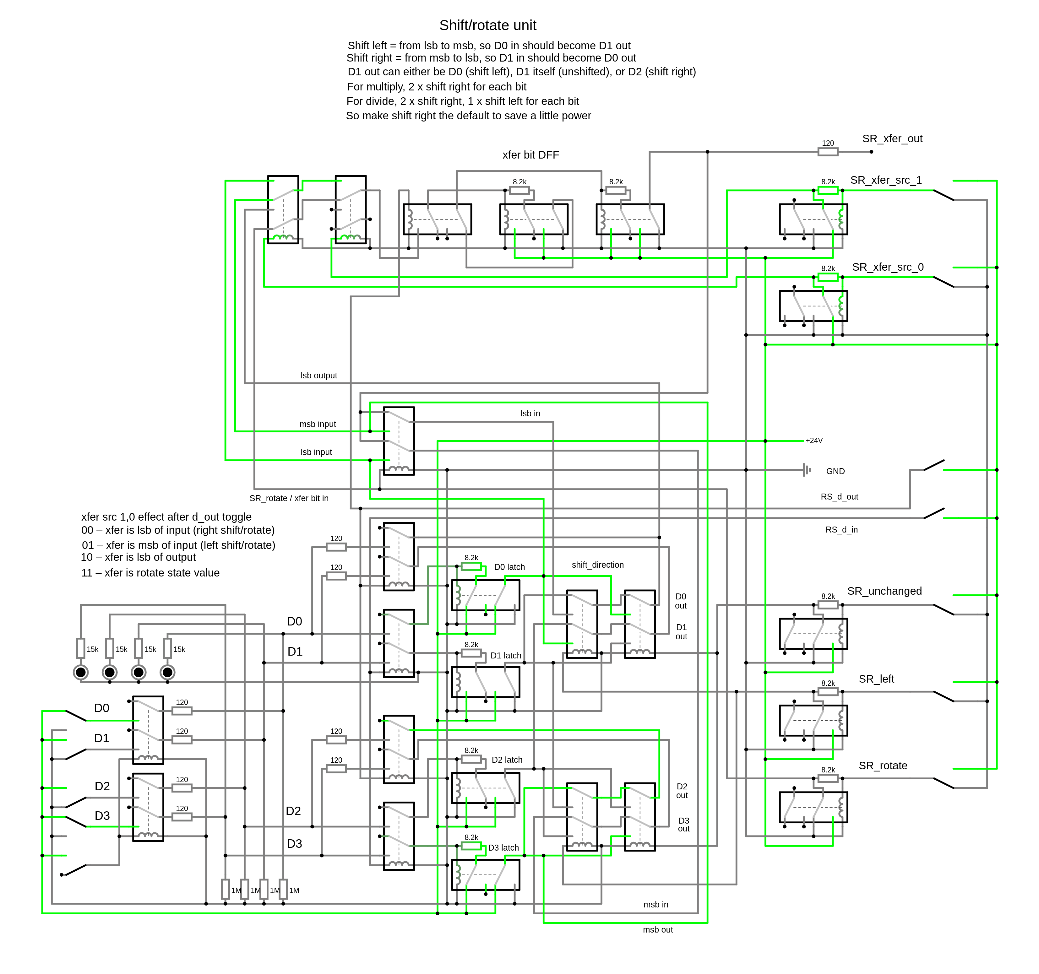
Shift /rotate unit
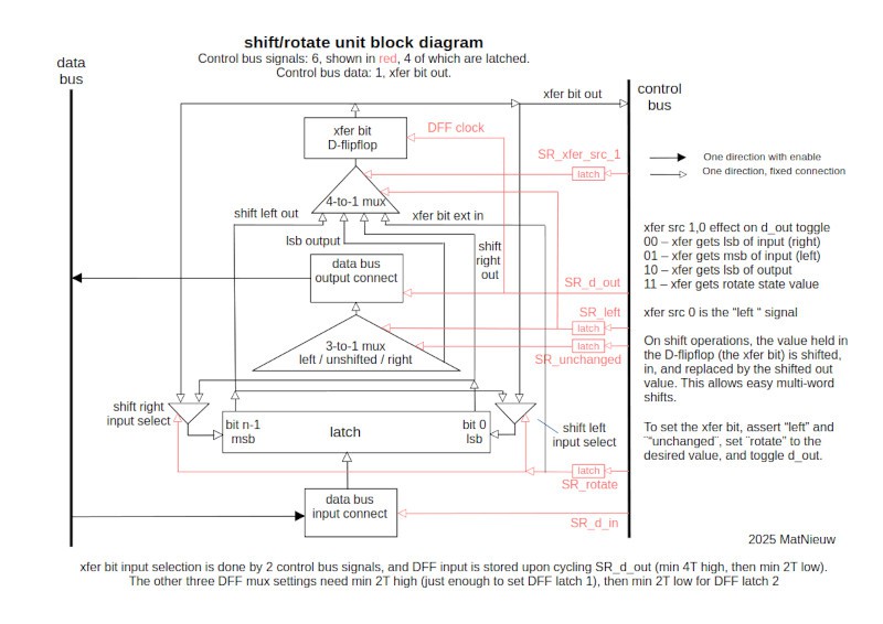
This 4 bit shift/rotate unit can do single- and multi word shifts, rotate, and also be used as scratch register. The input is loaded from a data bus and not changed, the output is selected bits from the input. The shift-in value comes from an internal D-flipflop, which can be set to 0 or 1 as desired, and normally gets set to the shifted-out bit at the end of an operation. For multi word right shifts, set the internal xfer bit, then shift the most significant word, then the least significant. For left, do the least significant first, then the most significant. For use as scratch register, the output is be the unchanged input.
Relays: 10 + 6 per 2 bits , DPDT only. Propagation time: 6T for load + retrieve changed value.
Control signals are shown with a latch, it is quicker without a latch but a latch saves relays in the control circuits (signals do not have to be kept active).
Relays are shown as 24V/2880 ohm, but can be any. For the latches and flipflop, see earlier latch description.
Note that signal d_out drives 1 + bits/2 relays, d_in drives bits/2 relays.
Signals driving the data bus have a self-resettable 100 mA fuse in series to limit current in case of logic failure (when one relay drives a signal line to GND, while another drives it to 24V). The schematic shows 120 ohm resistors, but that should be fuses.
A circuitjs simulation file is provided.
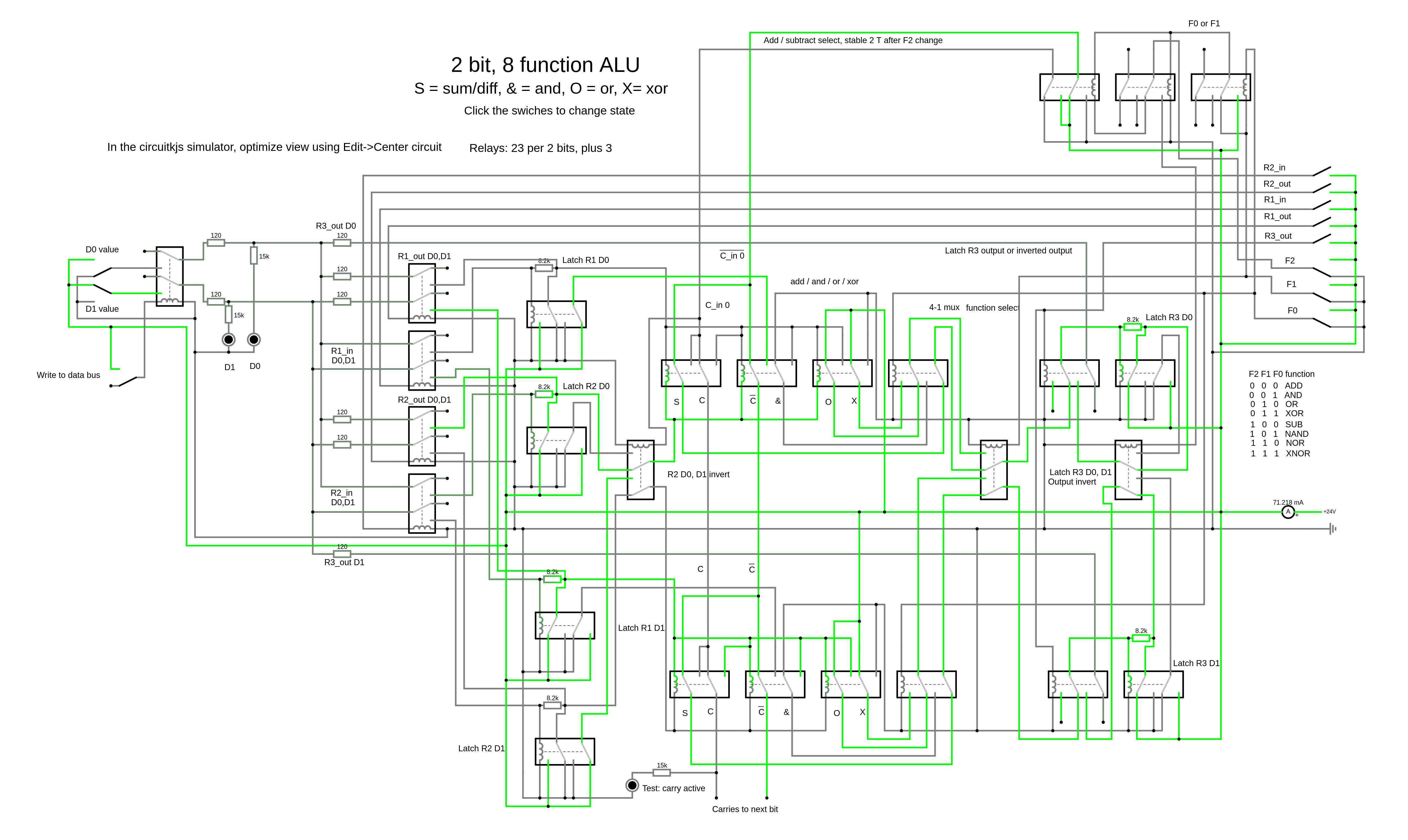
8 function ALU
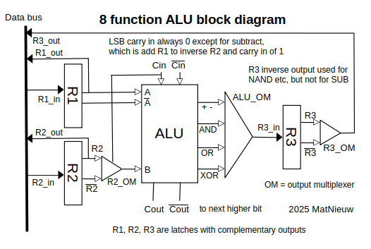
This 8 function ALU, here 2 bits, does ADD/SUB, AND/NAND, OR/NOR and XOR/XNOR in hardware. It has two input registers, R1 and R2, which can read from, and write to a data bus.
The central adder/logic part is an extension of J. Allen's clever adder, simply by having 3 relays in parallel, which give 4 functions, one of which is selected for the output. Subtract is always R1 - R2, where R2's output is inverted (one complement), and the carry of the least significant bit set to 1 (normally always 0). An internal register R3 is set to the result of R1 and R2 two relay settle times after the last R1 or R2 change. This register can write to the data bus too, its input is then disconnected and its output connected to the data bus. This way an operation like (R1 operation R2) to R1 is easily done without having to use intermediate storage.
Three function bits F0-F2 select the operation (see diagram below), where F2 enables the "negative" version of an operation, ADD becomes SUB, OR becomes NOR etc. Except for SUB, the inverse of the R3 value is used in the case (the latches have both normal and complimentary output).
It can be easily extended to any number of bits, connection the two carry outs from the previous 2 bits to the carry ins from the next higher two bits. Propagation time is always the same, even if you have 32 bits.
It uses 23 relays per 2 bits, plus 3, and uses 8 control signals. In spite of the number of relays, it is reasonable fast (for a relay ALU): an operation like 1) load R1 and select ALU function, 2) load R2, 3) wait for R3 to have the result and 4) write R3 to R1 can be done in 11 relay settle times.
You can load the circuit simulation in circuitjs (see Tools section), and play with the switches: use the left relay and switches to set write a data value to the data bus, then R1_in to put it into R1, do similar for R2, disable the left relay and use R3_out to se the result appear on the data bus. Use the F0-F2 functions to select the operation.
A circuitjs simulation file is provided.
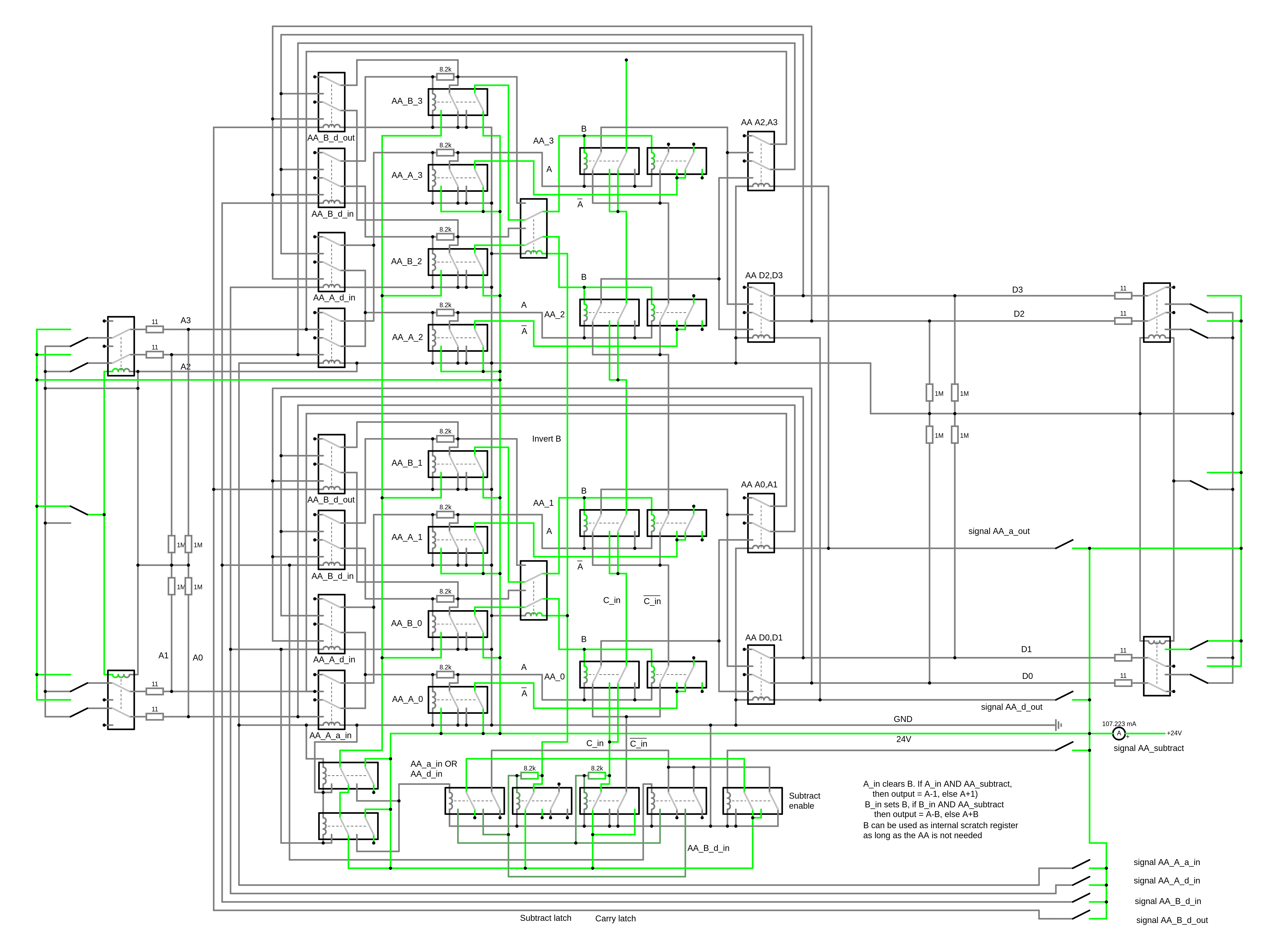
Address adder
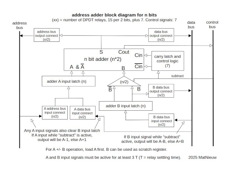
The address adder (AA) is a simple fast adder (based on J.Allen's fast adder), with 4 functions.
It saves relays if there are both a program counter and refresh counter (each of which would normally required their own incrementer), and the address bus is more than 8 bits wide, plus it allows computed addresses. It can also act as incrementer/decrementer outside the ALU.
It is intended to be connected to both an address bus and and equally wide data bus (e.g. 8 bits). It has two input registers, A (input from both address and data bus, no output), and B (input and output to data bus). There is no output register, the output can go to either address or data bus.
It has 4 functions:
a) A+1, the default if A is loaded, useful for incrementing a program counter, refresh counter, or stack pointer.
b) A-1, if A is loaded while the subtract signal is active, useful for decrementing a stack pointer.
c) A+B, if B is loaded
d) A-B, if B is loaded and the subtract signal is active.
The load signals need to be active for at least 3 T.
If the AA is not used, its B register can be used as a scratch register by the control logic.
The AA carry-out is exposed, with an ALU that allows external carry-in double word add/subtract can be done without using memory for intermediate storage.
A typical usage scenario during instruction fetch might be:
1. Connect PC out, AA A in, and memory address latch to the address bus.
2. After 3 T, disconnect PC out, AA A in, and memory address latch.
Connect PC in and AA output to address bus, after 2 T disconnect both.
3. PC has update address.
At the same time, the memory content can go over the data bus.
This AA requires 15 DPDT relays per 2 bits, plus 7.
A circuitjs simulation file is provided.