 Forthnutter
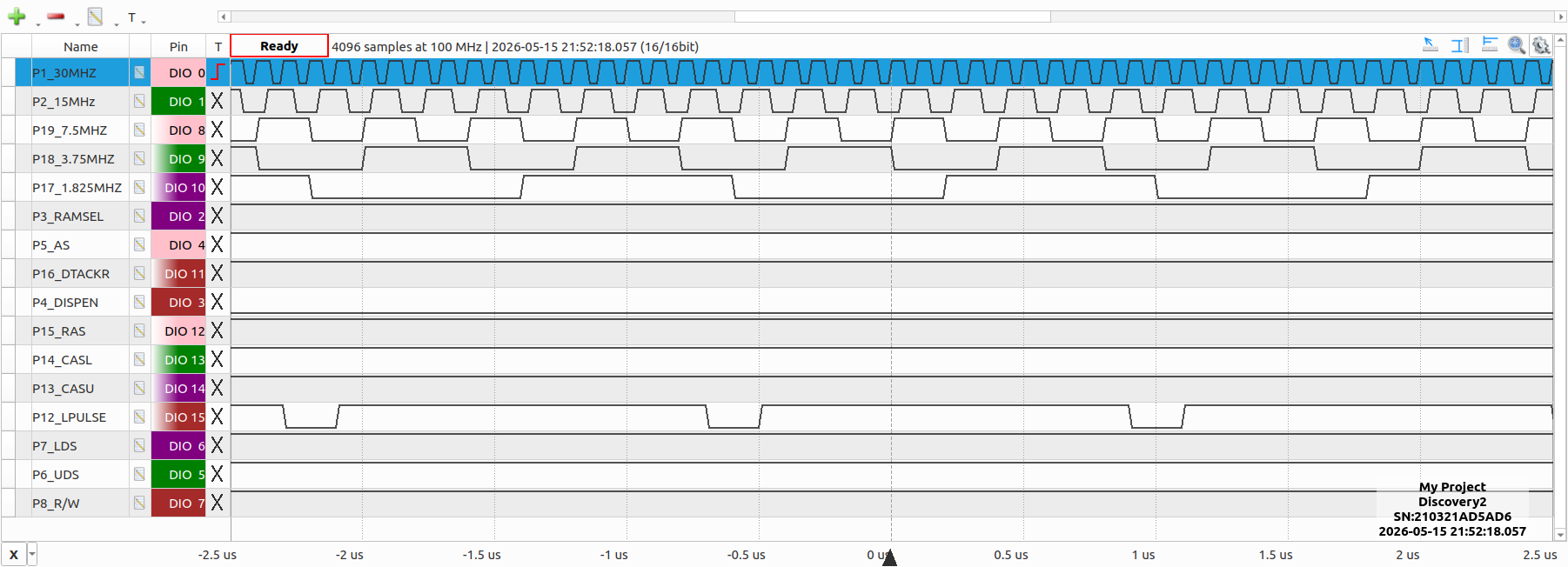
In the previous picture, I have made some errors on the analyser labels. I have removed the reset signal, i have run out of analyser inputs. I tied it to VCC not needed at this stage. I have been focusing on clock signal.
An interesting thing is the 1.825Mhz is out of phase with 3.75Mhz clock. All other clocks seems to clock on the rising edge.
I am will try and see if I can make the equation and simulate that with WinCUPL.
Discussions
Become a Hackaday.io Member
Create an account to leave a comment. Already have an account? Log In.
The 15, 7.5, 3.75 MHz signals are a binary counter. Internally, the values cycle from 0 to 7 but the outputs are inverted so they cycle from 7 to 0. The 1.875 MHz signal extends it to be a 4-bit counter, but it is deliberately phase-skewed so that it provides the right timing for use as the 6845 character clock. The falling edge is in the middle of the active-low LPULSE signal.
Are you sure? yes | no
Clocked at 30 MHz, the logic is a little obscured by the logic gate delays. A half cycle is 16.7 ns. The propagation delay of IC50a (a 74F74) is 3 to 7.8ns rising, 3.6 to 9.2 ns falling. Clocking at a lower speed, or even manually, would make the delays insignificant on a trace, and make the logic clearer.
Are you sure? yes | no