Jim Jagielski
-
Schematics - working draft
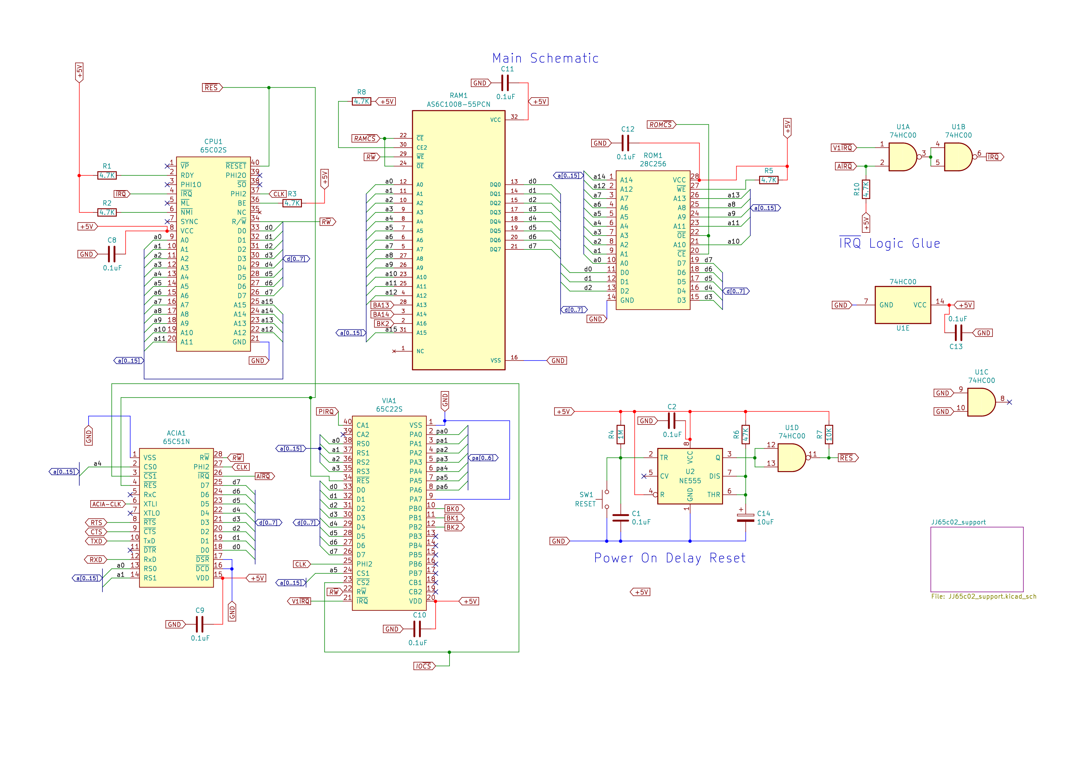
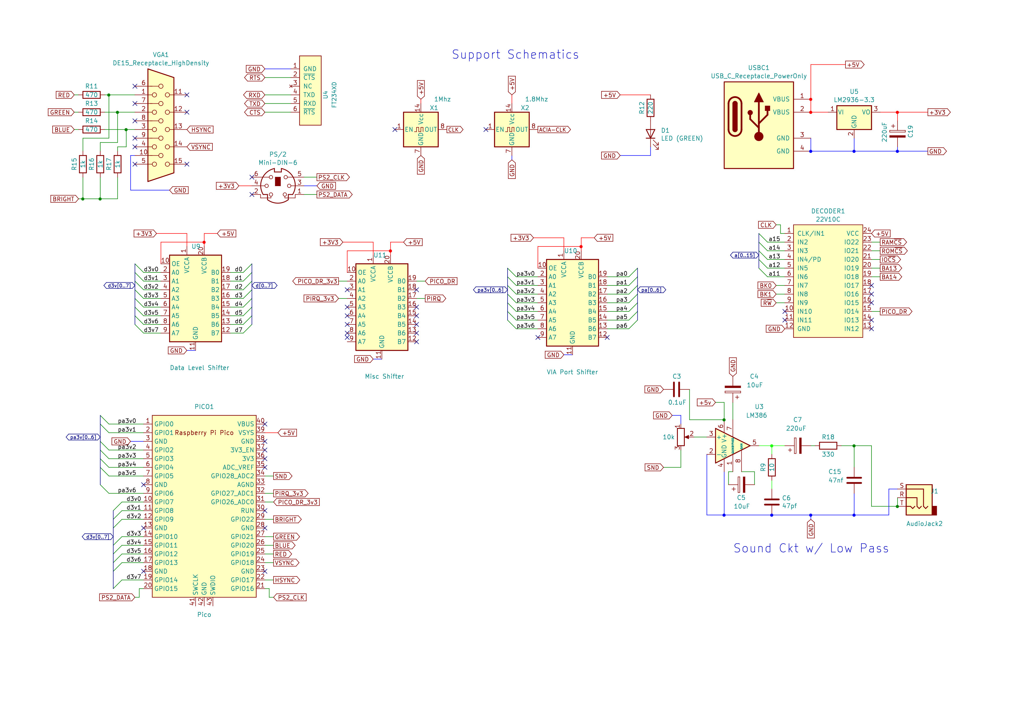
11/07/2023 at 19:57 • 0 commentsShort update. Worked on the schematic (Kicad7) and wanted to share the current version:
![]()
![]()
-
Quick Update
11/03/2023 at 12:47 • 0 commentsJust a very quick update since my last post.
It occured to me that I could simply use standard IRQ handling for the VIA input from the Pico (for PS2) instead of the CA/CB handshaking. This means that by dropping the handshake and moving to Interrupt handling, I now have one open pin to keep track of the 65C02 clock. Eventually, I may even decide to use the Pico to drive the clock, rather than just sense it. This again would reduce the overall chip count by one, and maybe add some flexibility. Plus, it wouldn't be a design change that makes what I do be incompatible with the standard BE6502 architecture (which is a goal for my project: I want whatever I do not be so specific to my design that nothing is re-usable by anyone else).
-
Raspberry Pi Pico for the win
10/31/2023 at 12:58 • 0 commentsAfter a lot of work and research, I decided to go with a RP2040-based option for my "specialized chip" and based on the availability of examples, as well as the price-point and the number of available GPIO pins, the Raspberry Pi Pico was the obvious winner.
My current design uses every GPIO pin, because I plan on using the Pico to also do PS2 keyboard functions, and get rid of the ATMEGA chip completely. Also, but using both PORTA and PORTB on a single 65C22 (VIA) chip, I can reduce chip count again.
The GPIO pinouts are as follows:
- 6 GPIO pins for VGA output (HSYNC, VSYNC and RBGI)
- 8 GPIO pins for communication to the Pico for VGA (directly connected using an I/O address)
- 1 GPIO pin for RD between 65C02 and the Pico (tells Pico to read data on the above 8 pins)
- 2 GPIO pins for PS2 Data and Clock
- 7 GPIO pins for PS2 ASCII data to VIA
- 2 GPIO pins for VIA handshake
It would be great if there was another pin available for the 65C02 clock signal, but I'm fresh out.
As far as the code is concerned, I'm working on the core VGA and PS2 functionality, and using PIO programming extensively. I found a great basis for the VGA library from a course taught by V. Hunter Adams from Cornell. Using his work as a guide, I was able to also figure out how to use PIO for the PS2 timing and scancode stuff.
Current versions of the code can be found at https://github.com/jimjag/JJ65c02/tree/main/Software/pico-code . I'll save a more indepth look at the code for another entry.
-
RP2040 choices
10/24/2023 at 18:32 • 0 commentsThe Raspberry Pi Pico or the Arduino RP2040
For VGA output, I was looking at either using a RP2040-based solution or a FPGA (likely the TinyFPGA BX). After giving it some more thought, and doing as much research as I could, I think I've settled on going w/ a RP2040 implementation. The reasons are:
- Price: Even the Arduino is less expensive that the TinyFPGA
- RAM: The RP2040 includes more RAM than the TinyFPGA
- Documentation: There are a lot more tutorials and projects already using the RP2040
This leads me to the next major decision: which RP2040 option to use?
Since I'm already including a different Arduino chip on my board, it would be nice to not have Yet Another Development Environment, and use the Arduino RP2040 Connect. Unfortunately, programming PIO on the Arduino is kinda wonky, requiring you to "compile" the PIO code using picoasm and then pull that resulting file into the Arduino IDE project. Workable, yes, but not ideal. Also, almost all PIO code assumes the Pico, and its pin layout. Do I really want to worry about that?
I also like the Arduino because it's a smaller, more standard form factor, which means it is easier to find chip sockets for it. But unfortunately, it is the more expensive option, by far, and includes functionality that I really don't need.
The Pico however is super cheap, and has a ton of already existing code and tutorials I could leverage. Its DIP size is weird, but that's just being picky. And from what I hear, the later versions of the Arduino IDE support the Pico natively (as a board). So maybe the answer is easier than I'm making it seem.
-
Address decoding
10/19/2023 at 15:41 • 0 commentsAs with most people, I started off with very simple address decoding, little more than "if A15 is 1, select ROM; if 0, select RAM". Breaking out space for I/O makes it a little more difficult, but depending on what address space you pick, even that can be easy (and by easy I mean "not requiring a lot of logic gates").
The problem is that this results in, at least in my opinion, a wasteful memory map. 32k of ROM seems way too much, and 32K RAM seems way too little. Carving out I/O space from ROM helps, but even then a simple implementation results in 16k or so just for I/O, which is extremely inefficient.
So I try to create a memory map that maximizes RAM, and minimizes ROM and especially I/O. My first real option was below:
MEMORY
{  ZP:   start = $0,    size = $100,  type = rw, define = yes;
  RAM:  start = $0200, size = $7e00, type = rw, define = yes, file = "%O.bin";
  IO:   start = $8000, size = $1000, type = rw, define = yes, fill = yes, fillval = $ea, file = %O;
  ROM:  start = $9000, size = $7000, type = ro, define = yes, fill = yes, fillval = $ea, file = %O;
}

SEGMENTS {
  ZEROPAGE:  load = ZP,  type = zp,  define = yes;
  SYSRAM:    load = RAM, type = rw,  define = yes, optional = yes, start = $0200;
  PROG:      load = RAM, type = rw,  define = yes, optional = yes, start = $0300;
  DATA:      load = ROM, type = rw,  define = yes, optional = yes, run = RAM;
  BSS:       load = RAM, type = bss, define = yes, optional = yes;
  HEAP:      load = RAM, type = bss, define = yes, optional = yes;
  CODE:      load = ROM, type = ro,  define = yes,  start = $a000;
  RODATA:    load = ROM, type = ro,  define = yes, optional = yes;
  RODATA_PA: load = ROM, type = ro,  define = yes, optional = yes, align=$0100;
  ISR:       load = ROM, type = ro,  start = $ffc0;
  VECTORS:   load = ROM, type = ro,  start = $fffa;
}
There are some problems with the above, namely that ROM is still a bit too big and you really can't access the higher addresses of RAM. The other problem is that the logic required to implement the above introduces some gate delays, even using faster AC chips, that limit overall system clock speed. It's obvious that improvements need to be made.
To handle both the complexity and the latency issues related to address decoding, I've moved to using a simple PLD, namely the Atmel ATF22V10C. I don't consider this "cheating" really, because I could easily use discrete chips if I wanted to, as long as I'm fine with clock speeds no faster than 4Mhz. But I like this solution for another reason: I can use CUPL to very easily design the logic.
Normally, you would describe the logic using standard boolean logic, but CUPL provides a much more clear and concise way. For example:
FIELD_ADDR = [A15..A00];
/* Address Decode Logic */
ROM       = ADDR:[B000..FFFF];  /* 20k */

IS_ROM = ROM;
CUPL is smart enough to generate the underlying logic.
This makes it easy as well to carve out space for RAM bank switching as well, with some signal pins determining if we are in the banked address space as well as which bank we'll be using. The current PLD file for WinCUPL is as follows:
Name     JJ65C02 ;
PartNo   00 ;
Date     10/6/2023 ;
Revision 01 ;
Designer Engineer ;
Company  jimjag ;
Assembly None ;
Location  ;
Device   p22v10 ;


/* Pin Map
       --------
PHI   |1     24| Vcc
A15   |2     23| /RAM_CS
A14   |3     22| /ROM_CS
A13   |4     21| /IO_CS
A12   |5     20| BA13
BK0   |6     19| BA14
BK1   |7     18| --
--    |8     17| --
--    |9     16| --
--    |10    15| --
--    |11    14| --
Gnd   |12    13| --
       --------
*/

/* Inputs:  From CPU*/

Pin 1  =  PHI;   /* 65C02 CLK */
Pin 2  =  A15;   /* Address lines from CPU */
Pin 3  =  A14;
Pin 4  =  A13;
Pin 5  =  A12;
Pin 6  =  BK0;   /* Bit 0 of the VIA 3-bit Bank number */
Pin 7  =  BK1;   /* Bit 1 of the VIA 3-bit Bank number */

/* Outputs:  Chip Selects */
Pin 23 = RAM_CS;  /* to RAM /CS pin */
Pin 22 = ROM_CS;  /* to ROM /CS */
Pin 21 = IO_CS;   /* to IO (VIA and ACIA) /CS pin */
Pin 20 = BA13;    /* To RAM chip, A13 */
Pin 19 = BA14;    /* To RAM ship, A14 */


FIELD ADDR = [A15..A00];

/* Address Decode Logic */

RAM       = ADDR:[0000..9FFF];  /* 32k */
BANK      = ADDR:[8000..9FFF];  /*  8k */
IO        = ADDR:[A000..AFFF];  /*  4k */
ROM       = ADDR:[B000..FFFF];  /* 20k */

IS_ROM = ROM;
IS_IO = IO;

!ROM_CS  = IS_ROM;
!IO_CS   = IS_IO;
!RAM_CS  = PHI & !IS_ROM & !IS_IO;

BA13 = (!A15 & A13) # (A15 & BK0);
BA14 = (!A15 & A14) # (A15 & BK1);
The goal is that the BK* pins will be driven by pins on the VIA chip. Schematics are being worked on.
-
Thoughts on Phase 2
10/13/2023 at 14:33 • 0 commentsI was quite happy with how Phase 1 of my JJ65C02 project ended up. I had a pretty solid miniOS coded up. I had ported EHBasic to not only my system but also to the (more robust) ca65 development system, and removed hard-coded addresses allowing it to be ported, and run, on any 6502-based platform. I also had full RS-232 capability and a working and solid YMODEM implementation that I could use to download pre-built binaries to RAM. I even had some rudimentary sound capability. All in all, I had taken this stage of the design where I wanted it to go. And so I was able to spend a LOT of time using the platform and running BASIC programs on it as well as native 6502 apps.
But as I did, I started getting the itch to start improving the hardware again, so much so that now I'm starting Phase 2 of the design in earnest. This promises to be a pretty significant change.
First of all, I plan on removing support for the LCD screen and the directional buttons. They take up a lot of real estate on the board and they simply aren't worth keeping around anymore. This means, of course, that I need a new primary user interface. Now I could continue to simply use the serial interface but I've come around and decided that the logical next step really is adding in PS2 keyboard capability and some level of VGA output.
My goal has always been to be faithful to the true retro nature of the project and so I've avoiding moving much capability to "modern", high-performance chips. But on the other hand, even old-school 6502 computers would used, when needed, specialized chips for video or I/O, and so it really doesn't feel like cheating all that much, if I handle the design carefully and in the spirit of retro. For the PS2 interface, since the design already includes a ATMEGA328, I'll leverage that. But the choice for VGA output isn't so clear.
I see 3 main possibilities:
- FPGA
- Raspberry Pi PICO
- Arduino Nano RP2040 Connect
Each has their own pluses and minuses, but I'll leave a more full discussion of all that for its own separate post.
The on-board speaker is also being dropped. Again, its a non-insignificant real estate hog on the PCB and I already have an audio jack output. I'll also be dropping the 9V input and move to a USB power port for native 5V coming in. And finally, I'll be likely moving from discrete logic chips to the ATF22V10C for the address decoding (and other signaling functions).
In addition to these "improvement" changes, I'm also going to add in support for RAM banking (8k banks) to support more complex programming requirements. This necessitates a change in the memory map (which is one of the reasons behind the move to the ATF22V10C) which I'm still mulling over. I'd like to have more than 32K RAM dedicated, but it makes the address and chip/bank selection logic quite nasty.
Off we go.
-
Some major details
10/12/2023 at 19:11 • 0 commentsHere's a quick summary of some details related to version1 of JJ65C02:
ROM-based BASIC:
I've planned on adding a ROM-based BASIC since the start, and now that the miniOS bootloader is "ready", I started the work in earnest. The question was, of course, which BASIC to use, with the top 3 contenders being EhBASIC (Enhanced BASIC), MS BASIC, and BBC BASIC. I decided on EhBASIC because it seemed the fastest and most capable, as well as having acceptable licensing terms (for non-commercial use). Unfortunately, the porting to the
cc65toolchain required some work.I used the KrisOS work-in-progress version as a starting point, which had already changed some of the zeropage assignments to the standard
.resformats. Unfortunately, there was still a lot of work needed to provide the correct spacing since EhBASIC loads some code chunks from ROM to RAM (in page0) and unless you have the spacing correct, you'll break everything. The fact that EhBASIC also re-uses the same zeropage allocations for different variables makes the situation even worse. So what I did was dump a full zeropage mapping of an unported EhBASIC and used that to work backwards on ensuring all variables and labels were where they were expected to be, regardless of where the starting point was.Once that was done, I jumped in on cleaning up the code and standardizing the syntax formatting. This involved lowercasing all opcodes and making sure that all labels used colons. After that, it was fixing CNTRL-C handing and then adding in an
EXITcommand to return from the Interpreter back to miniOS.Lots of work, but know there's an up-to-date version of EhBASIC ported to the
cc65toolchain for others to use and expand on! My little contribution to the cause.YMODEM:
I had already decided that I'd use the XMODEM protocol for that, mostly because there was a well-known and well-used 6502-based software implementation already available. But that implementation used XMODEM/CRC and, at least on the various terminal emulation packages I tried, there was really spotty and/or buggy versions of that. Either the host software used XMODEM Checksum or else there was something else, but I had failures at least half the time.
It wasn't all bad though, because while trying to track down the issues with XMODEM, I went ahead and implemented ACAI Rx IRQ handling; my thought was maybe it was overrun issues and buffering the input would address that. It didn't, but moving to an read buffer made sense no matter what. To make it super easy, I allocate 256bytes for the buffer, that way we automatically overwrite "old" data since the index pointers are 8bits and can just increment them and not worry about over-writing buffer space. And since my build doesn't include any hardware flow control, a read buffer is even more advantageous.
After some reasearch, it looked like YMODEM and ZMODEM were viable options, but the amount of work required for ZMODEM hardly seemed worth the effort. YMODEM is basically a formal improvement over XMODEM and so the vast majority of the existing code could be re-used. And I found that YMODEM support was both more ubiquitous and standardized. So YMODEM was it. And it works like a dream
Because of the read buffer, this meant that I needed to adjust my memory mapping again, although not the address decoder logic at all. I've set aside a full 768bytes for SYSRAM which give me some room for growth and allows me to finalize, at least for now, the starting address for RAM-based code.
Next on task was working out the specifics of assembling loadable RAM images using
cc65setup I have for building minios. The only real tricky part was in ensuring that the RAM code had access to the exported functions and memory block of the ROM code. There are 2 main ways of doing this.First of all, one could create an include file that defines the names of all such exports and associates them with their actual address.
cc65can create both a "label" file and a "map" file that includes such info, but not in an easily consumable format. That would would require some sort of small scriptlet that reads one of those files and creates aexports.hfile.The other is to simply have the build process for the RAM code link against the ROM code, and have
ld65do all that for us automatically. My first attempt was to archive all the ROM code object files into a library usingar65and link against that, but the indexing thatar65does messed up the addressing. So instead it links against all the individual object files, which works great, but is ugly. I've included a small example in the minios distro to explain the details and provide a template to follow.So at this point, both the hardware build and the software ROM has all the initial functionality I wanted, and it runs well and reliably up to 4Mhz.
The Current Memory Map:
The current memory map is as efficient and as functional as I could devise (currently, that is). The intent was to maximize RAM, and then ROM, and then ensure adequate set-aside for I/O.
To that end, the address and chip select decoder logic for RAM is super easy. If a15 is 0, then we're in RAM space, and we can use the full 32k. Alternatively, a15 high (1), means we are in ROM territory, but we also want to carve out a small chunk of that space for I/O.
For I/O, the design uses the
W65c22and thew65c51as the VIA and ACIA chips, respectively. Now most I/O, especially using these chip, don't need a large address space, and even 4K is excessive, but workable. To maximize ROM space, I use a74hc138and consider the states of address lines a14, a13 and a12. If these are all low (0), then, with a15 also low, that maps to the $8000-$8fff address space. We can use that as a chip select for the I/O chips; If any are high however, that means that we are in ROM space, and so we can use that as the other ROM chip select signal.So now that we are choosing the I/O chips, how do we determine which chip we actually want to enable? What I came up with is an elegant solution where address lines a4, a5,... are used for the secondary chip select. So, in this case, if a4 is high, we select the ACIA; if a5 is high, we pick the VIA. We can continue this way for up to 6 more chips. This leaves a3->a0 to select the actual address in these mini-blocks allocated per chip:
a11  a10  a9  a8  a7  a6  a5  a4  |  a3 a2 a1 a0  |    Address
  0    0   0   0   0   0   0   1  |   x  x  x  x  |  $8010-$801f
  0    0   0   0   0   0   1   0  |   x  x  x  x  |  $8020-$802f
  0    0   0   0   0   1   0   0  |   x  x  x  x  |  $8040-$804f
  0    0   0   0   1   0   0   0  |   x  x  x  x  |  $8080-$808f
  0    0   0   1   0   0   0   0  |   x  x  x  x  |  $8100-$810f
  0    0   1   0   0   0   0   0  |   x  x  x  x  |  $8200-$820f
  0    1   0   0   0   0   0   0  |   x  x  x  x  |  $8400-$840f
  1    0   0   0   0   0   0   0  |   x  x  x  x  |  $8800-$888f
Note that overlapping address spaces (like $8030, where a4 and a5 are both 1) are not used since this would select multiple I/O chips.
-
Moving to hackaday
10/12/2023 at 11:26 • 0 comments
JJ65C02
Working on my own version of a 65C02-based SBC. Everything is open source and permissively licensed.