Introduction
In this log, I'll explain in detail how this single-board computer works.
8 bits bus only
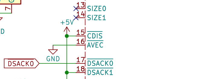
The 68020/68030 have dynamic buses; this means that they are not fixed to 32 bits. A 68020 board can have 32 bits RAM, 16 bits ROM, and 8 bits IO. Of course, this flexible bus is great, but it also makes things complicated. The CPU asks for one, two, three(!), or four bytes, and the board responds with what it can deliver. The lines SIZE0 and SIZE1 determine what the CPU is asking for. The lines /DSACK0 and /DSACK1 determine what the board can deliver. It is clear that a lot of logic (PAL) is needed to decode that.
Since my design needs to be as simple as possible, only a (fixed) 8-bit bus is needed. Therefore, SIZE0 and SIZE1 are not needed, and only /DSACK0 needs to be asserted (to zero). Since this also determines the wait states, this signal is coming from the wait state generator. /DSACK1 is always high.
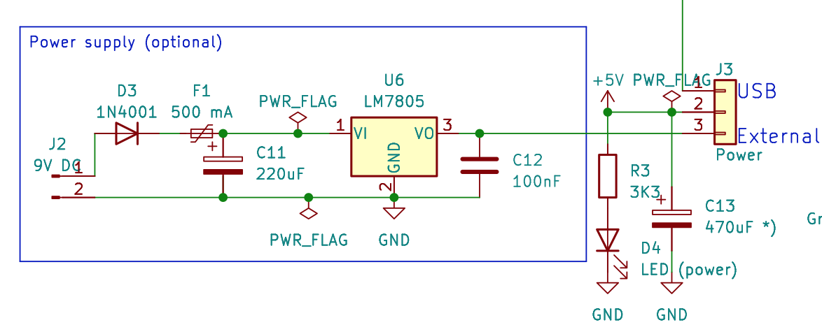
Optional power supply
There is room for an optional power supply, using the good old 7805. It is capable of 1.5A, more than enough. It also has a 500 mA polyfuse to prevent damage during the device's construction. Perhaps it's better to use a 250 mA while testing. The diode (D3) prevents damage if the power is accidentally reversed.
Via a header/switch, it is possible to draw power from the USB serial interface or using the power supply. If you are using USB power, it is better to add the 470uF capacitor (C13). While using the LM7805 regulator, this is not necessary.
Clock, reset and halt-circuit
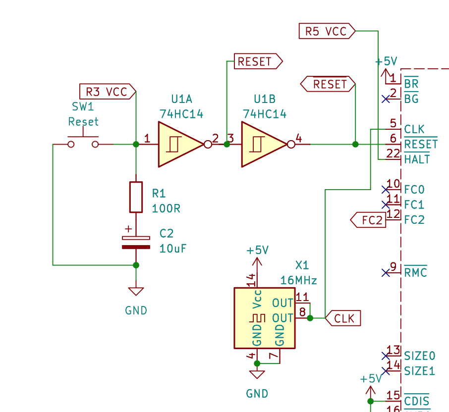
- The clock is provided by a crystal oscillator; the footprint is modified to accommodate both half-can and full-can oscillators. Place it on a (self-made) socket, and you can easily experiment with different clock speeds. The clock speed can range from 8 to 25 MHz in normal operation and up to 40 MHz for overclocking.
- The reset circuit is somewhat simplified. A simple R/C combination generates the reset pulse, and the Schmitt trigger (74HC14) transforms it into a nice digital signal. The RESET-signal (U1A) is fed to the UART 16550. Officially, the CPU /RESET line is also an output, but it is only asserted when the processor executes the RESET instruction. I have never needed a software reset pulse. Therefore, I decided to treat the CPU /RESET-pin as input only (In theory, it can be damaged if /RESET is continuously asserted from the CPU).
- The /HALT pin is held high with a 10K resistor.
Address decoder
The 74HCT139 is my favourite chip: for decoding ROM, RAM, IDE and UART, only half of the IC is needed. A0/A1 (pin 2/3) from the decoder are connected to the address lines A19/A20 of the CPU, and the /Enable (pin 1) is connected to the /AS (address select). That's all to generate the active low chip select lines for ROM, RAM, IDE and UART:
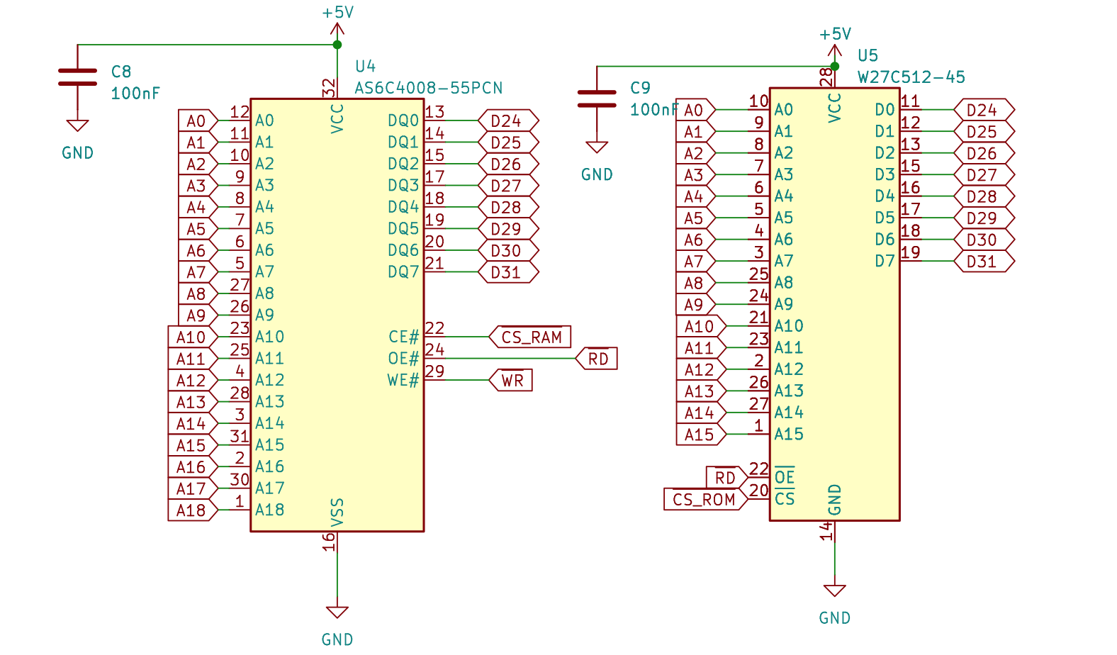
- /CS_ROM: 0x00.0000 - 0x00.FFFF (64KB EEPROM)
- /CS_RAM: 0x08.0000 - 0x0E.FFFF (512KB RAM)
- /CS_IDE: 0x10.0000 - 0x10.0007 (IDE/SD-card connector)
- /CS_UART: 0x18.0000 - 0x18.0007 (UART)
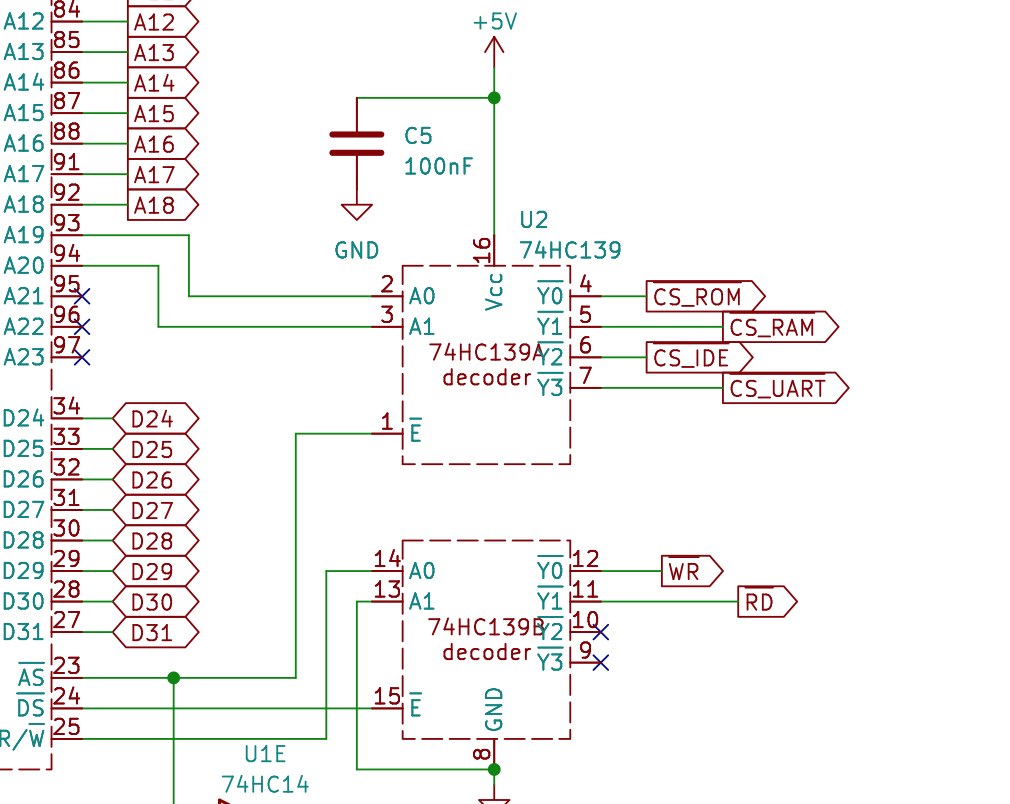
/READ and /WRITE
The other half of the 74HCT139 is used for generating the /RD and /WR signals. These signals can also be generated with a simple inverter, but they are only active if /DS (pin 24) is asserted. Since there are no inverters left, this is a nice solution.
RAM and EEPROM
Now we have generated the base signals, connecting RAM and ROM is straightforward. The data lines D0-D7 from the RAM/EEPROM are connected to the datelines D24-D31 of the CPU. This needs some explanation: this design uses an 8-bit data bus. Since the 68000 family is big endian, the highest data lines from the CPU are used. D0-D23 are not connected.
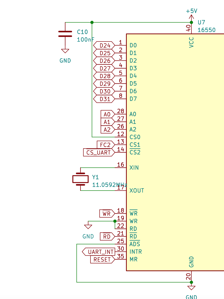
UART (CPU side)
The connections to the 16550 UART to the CPU are as straightforward as the RAM. Some extra signals:
- There is an additional chip select (CS1) on this chip; it is connected to the function code FC2 signal. FC2 is high if the processor is in supervisor state. In user mode, this signal is low, so user programs can't read or write to the UART/IO. This protects the system from malfunction. Be aware of this behaviour if you write programs.
- Xin and Xout (pins 16 and 17) are connected to an 11.0592 MHz crystal. The 16550 has a oscillator on board. Adding this extra crystal makes the baudrate independent from the CPU clock.
- Pins 19 and 22 are additional RD and WR signals and should be connected to the ground. In my initial schematic and PCB, I made a mistake and connected them to Vcc. Therefore, you can observe a correction in the pictures of my PCB. This has been rectified in the published schematic and PCB.
UART - IO
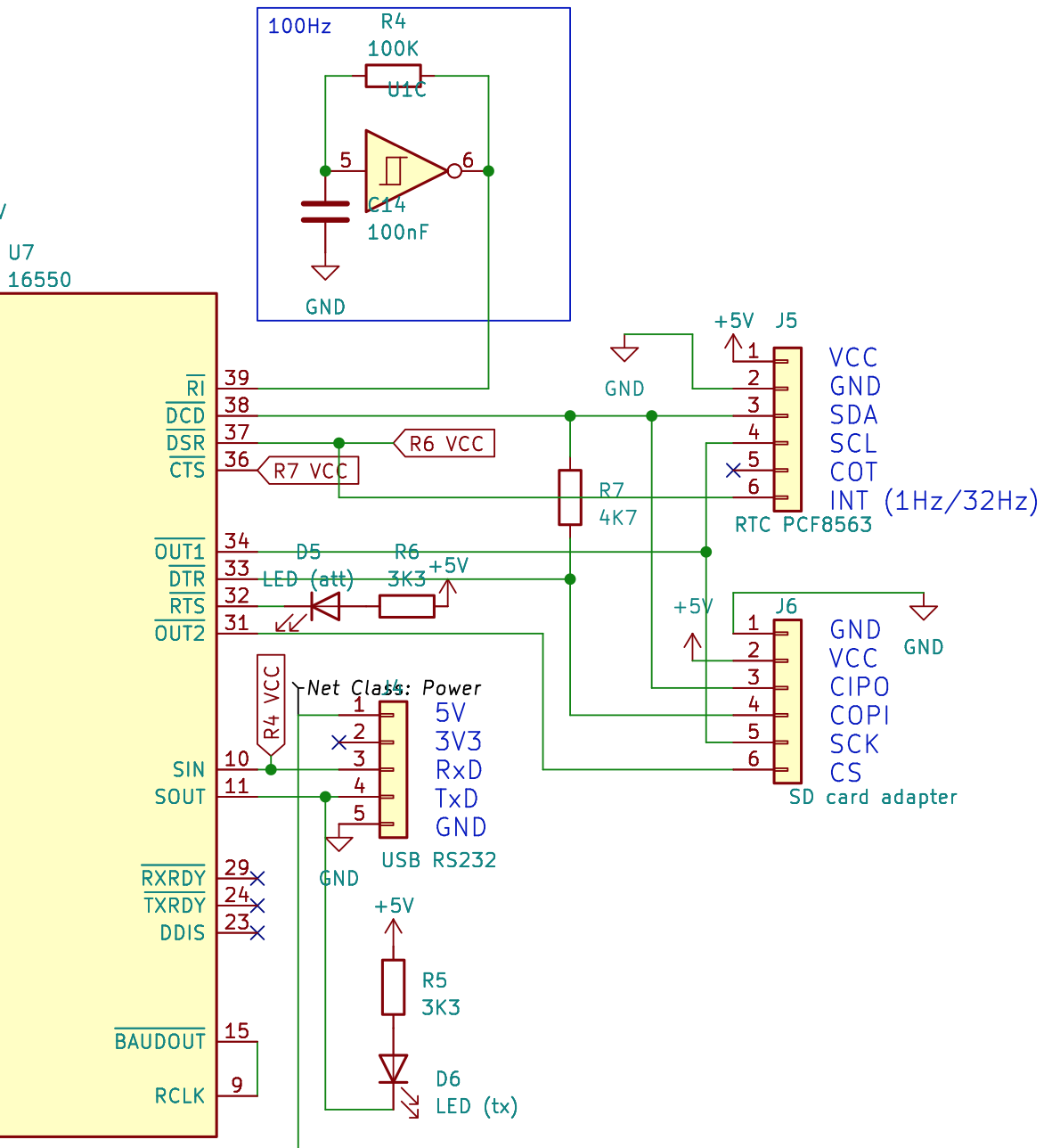
The 16550 UART has beside the serial in (SIN) and serial out (SOUT) four input and four output lines. These pins are used for software generated SPI and I2C. In a previous design (68000 minimal homebrew computer) I used a 6522 VIA, which has programmable input/output lines, ideal for I2C; the data line SDA is both input and output.
The 16550 has only fixed input and output lines, so I had to combine these with resistors to create the data line for I2C. Also the lines from SPI and I2C are combined. Take care in the software not to send data to both peripherals. I haven't tested this yet!!!
SPI (SD-card)
- OUT2 is connected to the /CS (chip select).
- OUT1 is connected to the /SCK (clock).
- DTR is connected to COPI (controller out, peripheral in).
- DCD is connected to CIPO (controller in, peripheral out).
I2C (for RTC PCF8563)
- OUT1 is connected to SCL (clock).
- DTR (output) and DCD (input) combine to the SDA signal (data).
- DSR is for generating interrupts from the clock (INT).
100 HZ oscillator
- /RI (p39/input): connected to a simple 100 Hz R/C oscillator. This generates periodic interrupts for timing and task switching.
Signal LED
- RTS is connected to LED D5 for signalling and trouble shooting.
USB serial
- SIN and SOUT are connected to the USB serial module. This module can optionally provide the board with power.
IDE/SD-card adapter
I found this IDE/SD-card adapter on the internet for less than €10. It is a 44-pin IDE-compatible card using an SD card. Because it is IDE-compatible, it is easy to use and could be ideal for home-brew computers. It should also be compatible with the 8-bit bus, but I have no idea if this is going to work in my design.
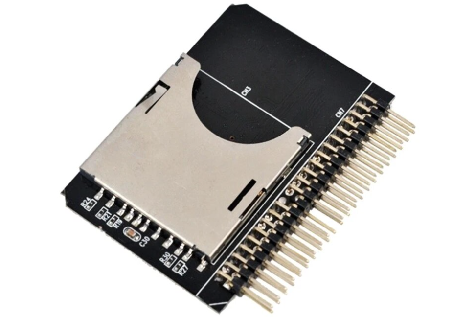
So this is the connector for it. (It cannot be used for CF cards because these cards use 16-bit data transfer, and in this design, there is only an 8-bit data bus.)
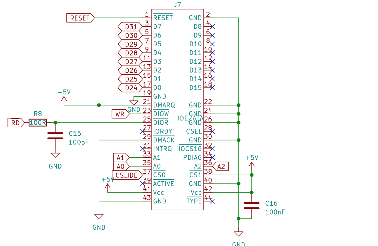
- /DIOR is for reading data. There are a timing problems with this; first, the /CS0 has to be asserted, and then the /DIOR (used for latching out the data). In the 68000 family, both signals are active at the same time. Perhaps the particular card doesn't mind, and if needed, the read signal can be delayed with a resistor and capacitor. Of course, the latter is not a good design.
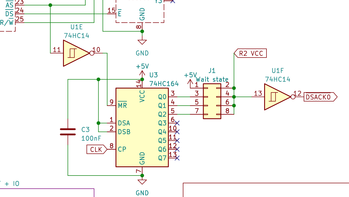
Wait-state generator
For higher clock speed, it is desirable to add wait states for the RAM/ROM and IO. It is surprisingly simple to generate these with a 74HC164 shift register.
- DSA/DSB are high so ones are shifted out.
- /MR is connected to the inverted /AS (address select), so when a read/write cycle starts (/AS is low) the reset is cleared and shifting begins.
- CP is connected to the CPU clock.
- The outputs (Q0 - Q2) has to be inverted, because /DSACK0 is low active.
- With a header/switch you can choose for zero (Q0), one (Q1) or two (Q2) wait states.
- The 10K resistor R2 VCC makes the whole chip optional (zero wait states).
Unfortunately I made a minor mistake; Q0 is zero wait state while I expected one. So the description on the PCB is wrong.
Discussions
Become a Hackaday.io Member
Create an account to leave a comment. Already have an account? Log In.