I'm beginning to reverse engineer the protocol used by the LCD controller. I think this is simply prefaced by a memory address and then the binary values for which segments of the LCD should be turned on. If I'm right, the memory address will always be the same, and it's just a matter of correlating which segments are on with which bits are written to each register..
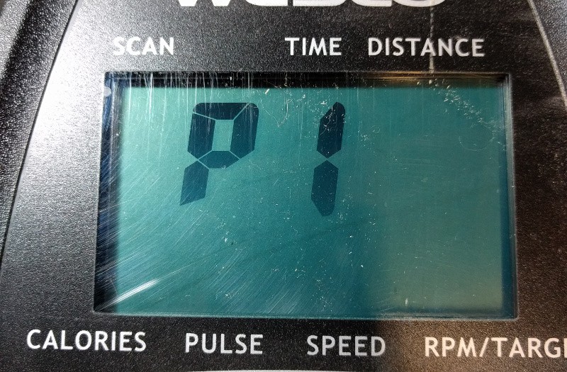
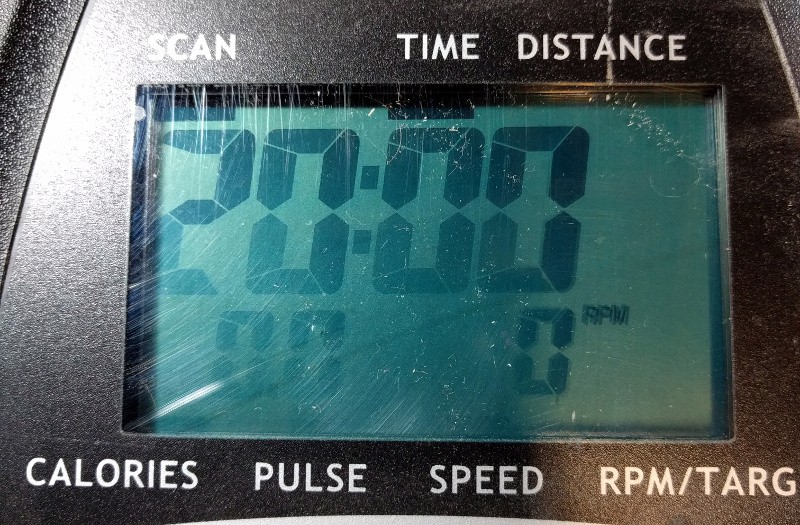
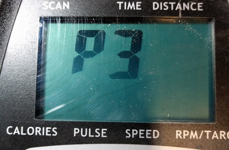
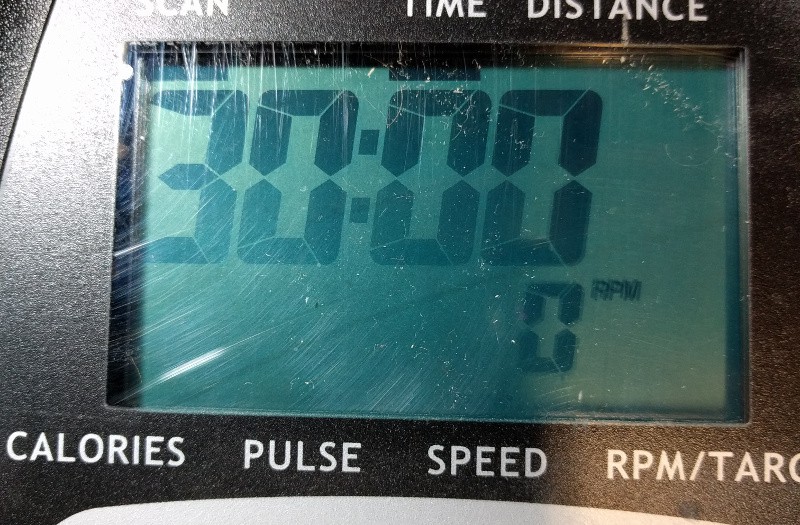
Here are four screens to get me started:

Preprogrammed exercise 1 splash screen. Captured output:
0xA0, 0x00, 0x00, 0x00, 0x00, 0x03, 0x98, 0x28, 0x00, 0x00, 0x00, 0x00, 0x00, 0x08, 0x00, 0x00, 0x80

0xA0, 0x00, 0x00, 0x00, 0x06, 0xDF, 0xAF, 0xEF, 0xA8, 0x40, 0x07, 0xA9, 0x20, 0x00, 0x00, 0x00, 0x00

0xA0, 0x00, 0x00, 0x00, 0x00, 0x03, 0x9E, 0x98, 0x00, 0x00, 0x00, 0x00, 0x00, 0x00, 0x80, 0x00, 0x00

Timing screen for preprogrammed exercise routine 3. Captured output:
0xA0, 0x00, 0x7E, 0xFA, 0xC4, 0xFF, 0xAF, 0xEF, 0xA8, 0x40, 0x07, 0xA9, 0x20, 0x00, 0x00, 0x00, 0x00
I'm just now starting process some of this data to figure out if it is a direct bit-to-segment mapping (which I think it is). Take these early samples with a grain of salt. I might have an off-by-one error on the pictures I took versus the data samples I snapshotted :-/
I'll update this log as I go.
I am optimistic that this will be a straightforward process. Looking at the timing diagram for continuous writes I should be in good shape. The leading bits should be 0b101 (write) 0bxxxxx (address) so 0xA0 which we have for each sample is "Write to register 0"

 Mike Szczys
Discussions
Become a Hackaday.io Member
Create an account to leave a comment. Already have an account? Log In.