 sky-guided
It's been a busy couple of months behind the scenes -- this project is basically finished! I'll be breaking the final few updates into a couple posts, while I wrangle loans of camera equipment for the beauty shots.
Circuit Unification
Taking the different prototyped modules and banging them together:
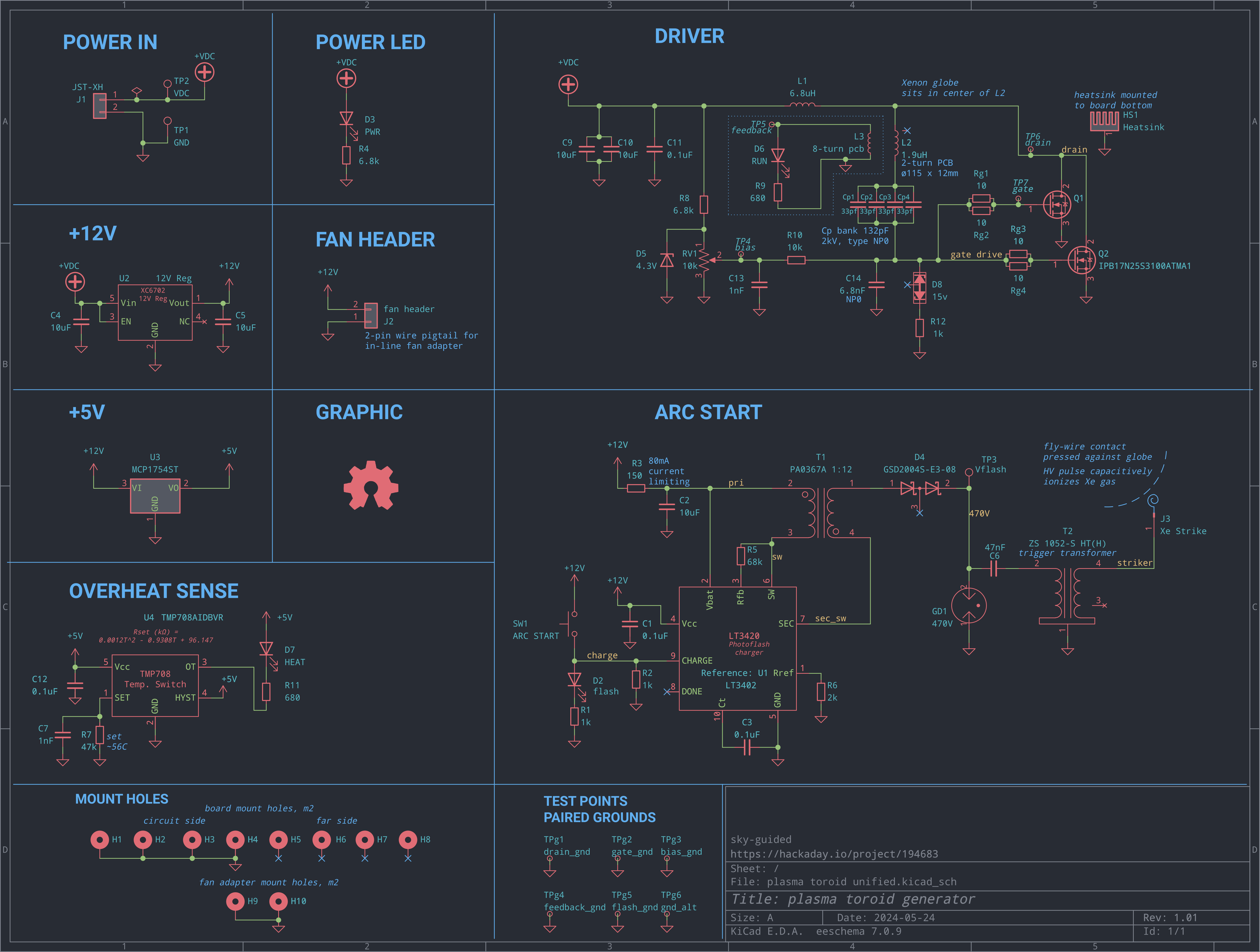
(you might have to click to embiggen)
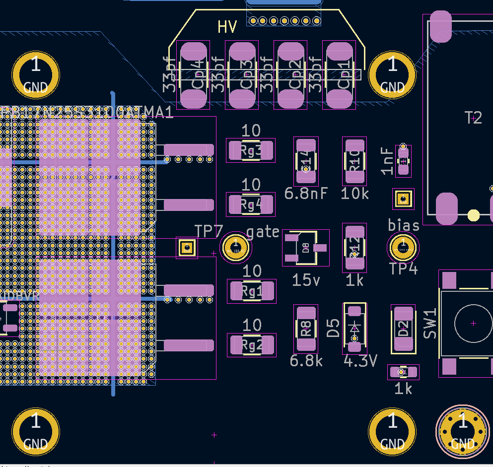
I've paralled the mosfets for better heat dissipation. This doesn't help quite as much as one would like (since a lot of the losses are switching and not resistive), but it does help. The mosfet gate resistors are also paralled since they get quite hot before the arc is struck. I'm not sure why that behavior is occurring -- if you know, drop me a line!
The 4.3V zener diode (D5) for regulating gate bias is a carefully chosen value for this particular mosfet and circuit. Cranking the knob full-clockwise guarantees oscillations start, but doesn't set the bias so high as to cause excessive power draw and heating. The use of full knob range also makes adjustments more precise and controllable.
A bank of four 33pF capacitors is a balance between heat distribution and board space. While the board itself has plenty of room (see below), I ran into some odd layout constraints due to things like the under-board heatsink mounting holes. The cabs do get pretty hot before the arc is struck, but are plenty cool during operation.
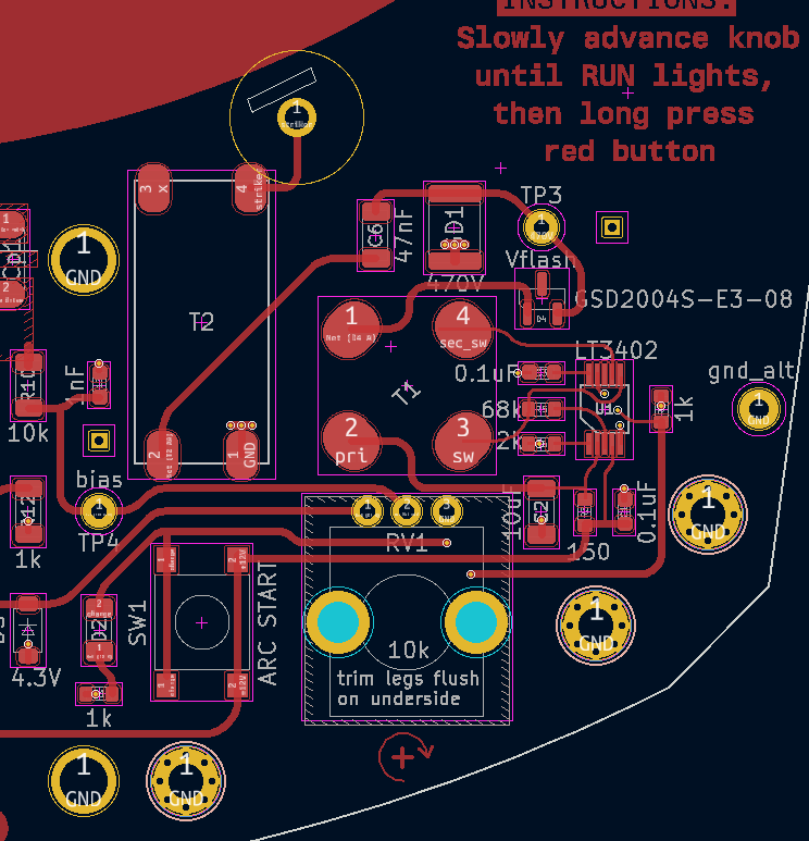
There's a total input bulk capacitance of 30μF (shown as two caps on main power and one before the 12V regulator). Less bulk capacitance caused occasional power supply brownout/shutdown.
The oscillation sense coil from Update #6 has been brought on-board, shown in the dotted area within the main driver section.
Arc start is basically the same as discussed in Update #7. I keep waffling on whether a GDT value of 300V or 470V is preferable here -- 470V may be shown, but keep your mind open.
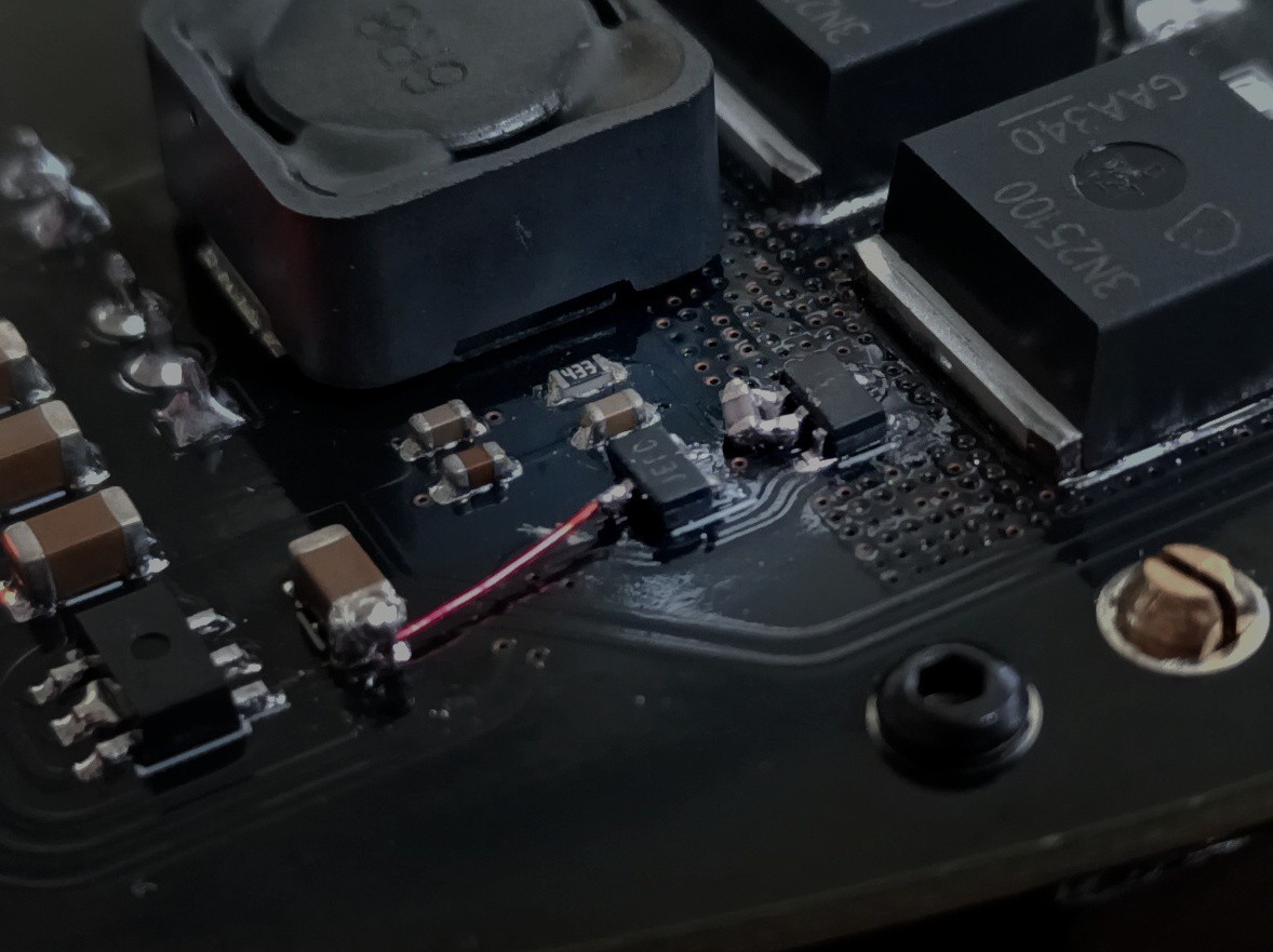
The only real new addition is the overheat sense. There's nothing special here; it's almost exactly per the datasheet for the TMP708 IC. The one bit of oddness was having to add a small decoupling capacitor in parallel with the programming resistor, because the overheat IC was placed as close as possible to the mosfet drains and it was picking up EMI. Debugging that was fun -- while poking around with scope probes, I noticed that merely touching the sense pin fixed the problem.
Here's a delightfully goofy photo from a prototype board, showing a 0603 capacitor bodged directly on to the IC pins:
Programming a trip value of ~56C was about right for raising alarm when the mosfet case temperature hit 100C.
PCB Design
An overview:
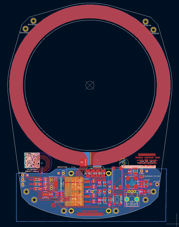
Details might not be super visible at this far out a zoom, but here's the overall layout. Power input and status LEDs are far left, overheat sense is lower center-left, main driver is center (with knob lower center-right), and arc start is far right. The heatsink is mounted to the board bottom, outline indicated by the cyan square around the center area.
Most of this layout is relatively low-density. The minimum size was constrained by needing to fit a heatsink underneath which could accomodate a 40mm fan. There's a handful of components which are 1206-sized even though 0603 would have worked, simply because that larger size looked better.
The rounded traces were made using the KiCAD plugin "round traces".
MOSFETS were placed on a large copper fill, stitched to the heatsink on the bottom with a lot of thermal vias. The thermal tab on the mosfet is attached to Drain (and not GND), so rather than having truly a massive cut in my backside ground plane for the backside Drain copper pours, I split the drain pours into smaller sections with cruciform GND traces.
The TMP708 overheat sense IC was put within a small cutout on the thermal fills, to maximize thermal coupling. A SMD thermal jumper would have been "better" but I didn't want to add it to the BoM.
The main driver section in the board center is arranged to prioritize visual symmetry. One detail here is that each test point has a paired ground point to make probing easier. (This project is really sensitive to interference from large loop areas on probe leads!)
A cutout under the primary capacitor bank isn't directly for high-voltage creepage/clearance reasons, but mostly to allow for picking up any excess solder balls or flux residue and is recommended by TDK as best-practice for higher voltage SMD caps.
The far right side of the board hosts the arc-start portion of the circuit. It's mostly notable because I didn't give quite enough clearance for the high-voltage arc start fly-wire contact (J1, visible inside the yellow circle near the top). It's prone to arcing over to the primary inductor. I don't think that's going to hurt anything but it doesn't feel great -- conformal coating or a dab of hot glue might help.
I am going to open-source this project as soon as I finish this round of update blogs.
Physical Design
Since the start, a key goal was to have a finished product that didn't look like a workbench prototype.
Here's what I came up with:
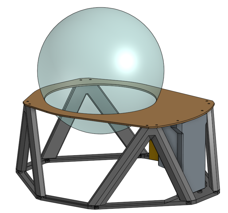
Rather than the "layer cake" of most folk's designs, I'm going for something more reminiscent of early 20th century engineering.
Early drafts included a lasercut or printed no-finger-poking safety shield over the electronics, but I decided it looked terrible. Please don't touch the zappy parts.
Components are printed as individual flat pieces, and attached together with heat-press inserts and M2 screws. While a single-piece print would be possible, using multiple parts allows stronger layer-line orientation and avoids print head jump moves which can visibly affect surface quality.
The blocky section in the front-right is a shroud to cover the heatsink (mocked up in blue), and an attachment point for the (brown) 40mm fan. The USB-C power supply module screws down to two of the four semi-conical mounting points.
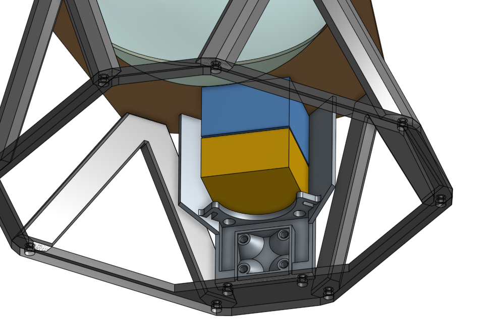
While I'd have preferred to have the USB-C-PD power supply integrated on to the main board, availability for USB-C-PD trigger ICs in the is currently terrible within the United States. I've decided to use the Adafruit HSUSB238 power delivery dummy breakout as a standalone module. It's a touch larger than some others out there, but it has mounting holes. A standalone board does allow plugging a USB cable in at closer to desk surface height, which in my opinion is a bit nicer.
Coming in the next update: an excessively fancy circuitboard, sponsored by PCBWay.
Discussions
Become a Hackaday.io Member
Create an account to leave a comment. Already have an account? Log In.
If you want to add USB-PD on the board that you can order from the US, check out AP33771 IC from Diode. My work uses a different IC but would recommend this for the similarity to HUSB238
Are you sure? yes | no
Oh rad, thank you! It's a bit late for this project (and it's unfortunate I didn't find this chip when searching), but I'm absolutely going to be putting similar functionality on future projects.
Are you sure? yes | no
Also, I have some projects that found an easy way to negotiate variable voltage from a USB-C brick using PPS. Just in case you have any idea for utilization.
Are you sure? yes | no