 sky-guided
For the final build of this project, I wanted something special.
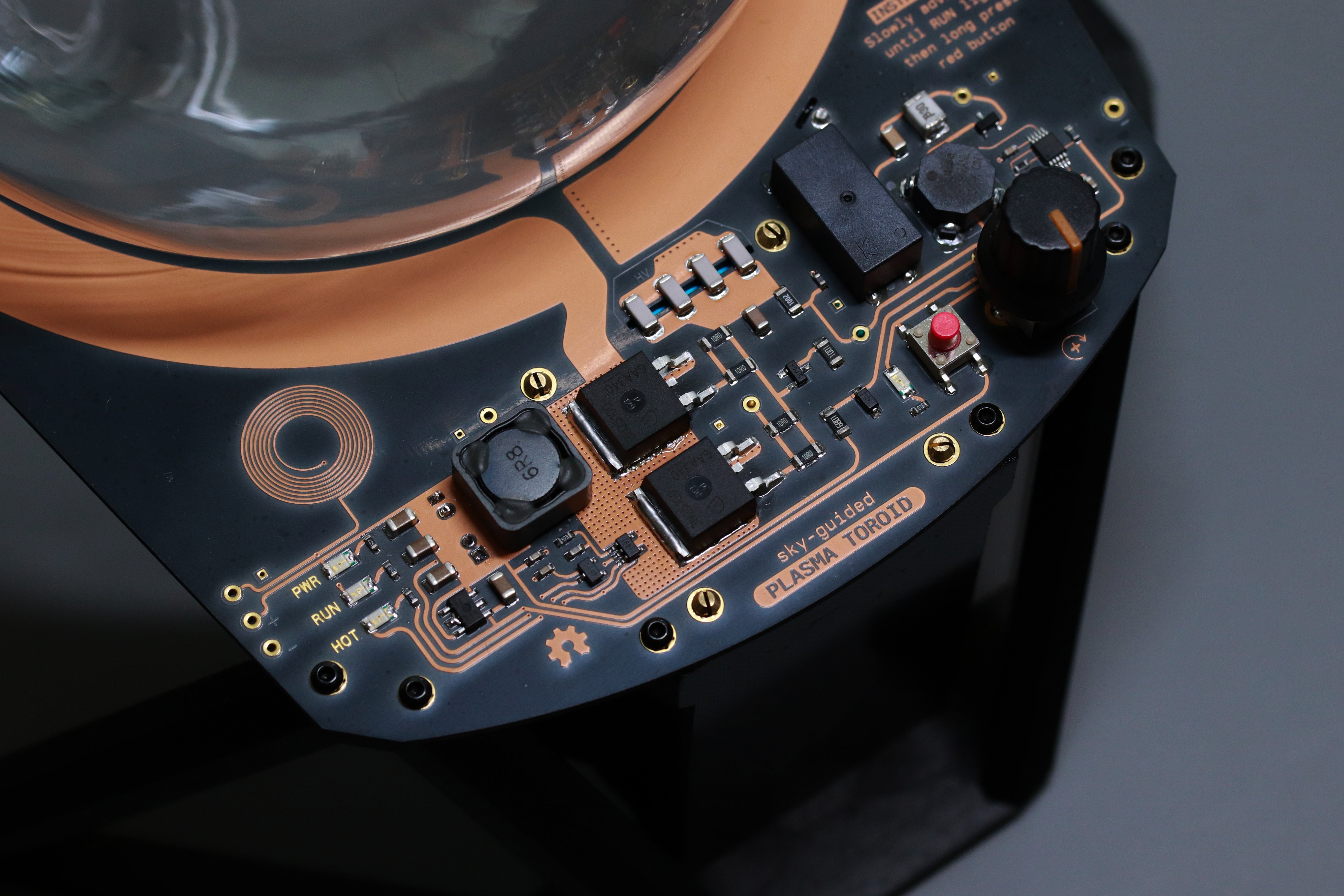
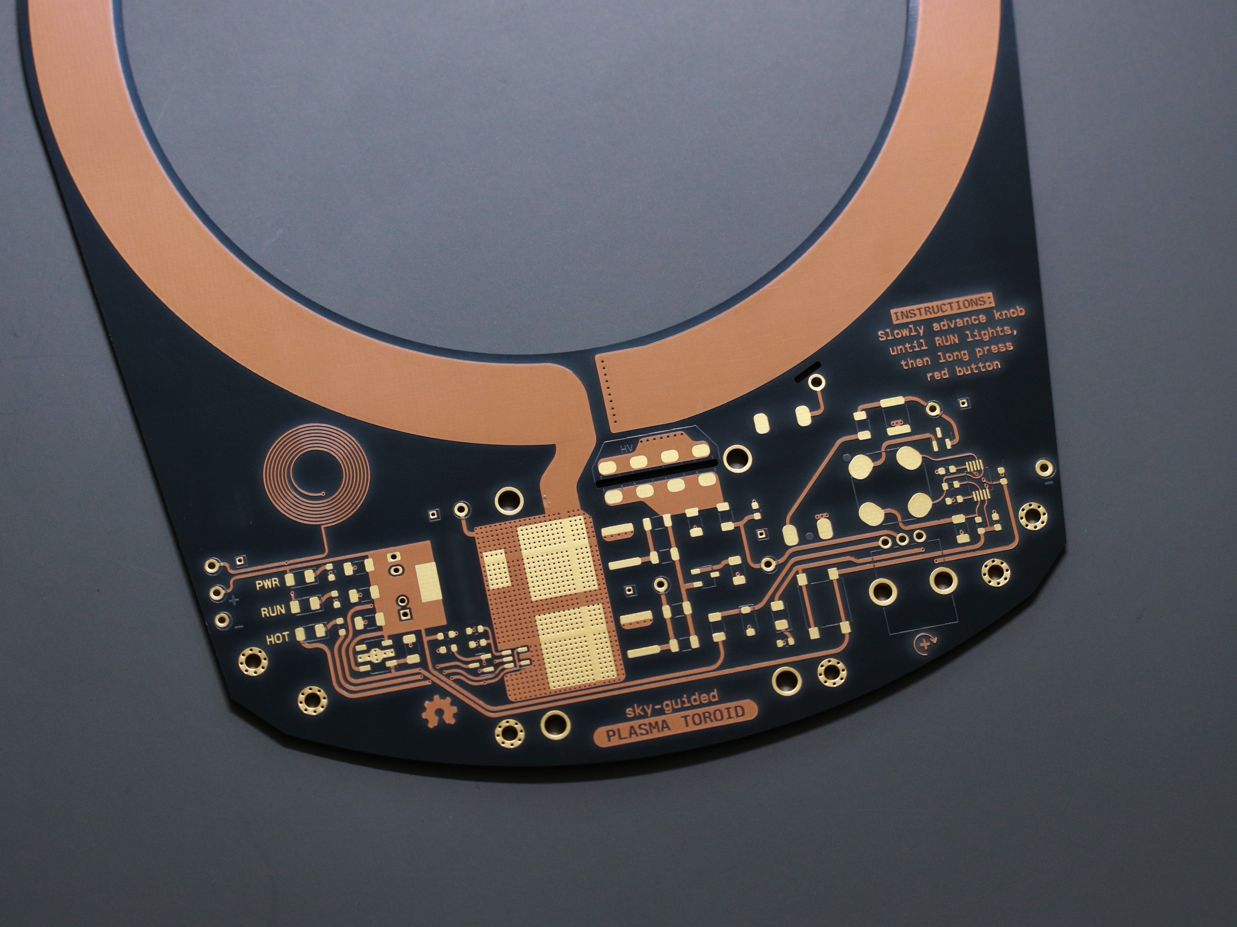
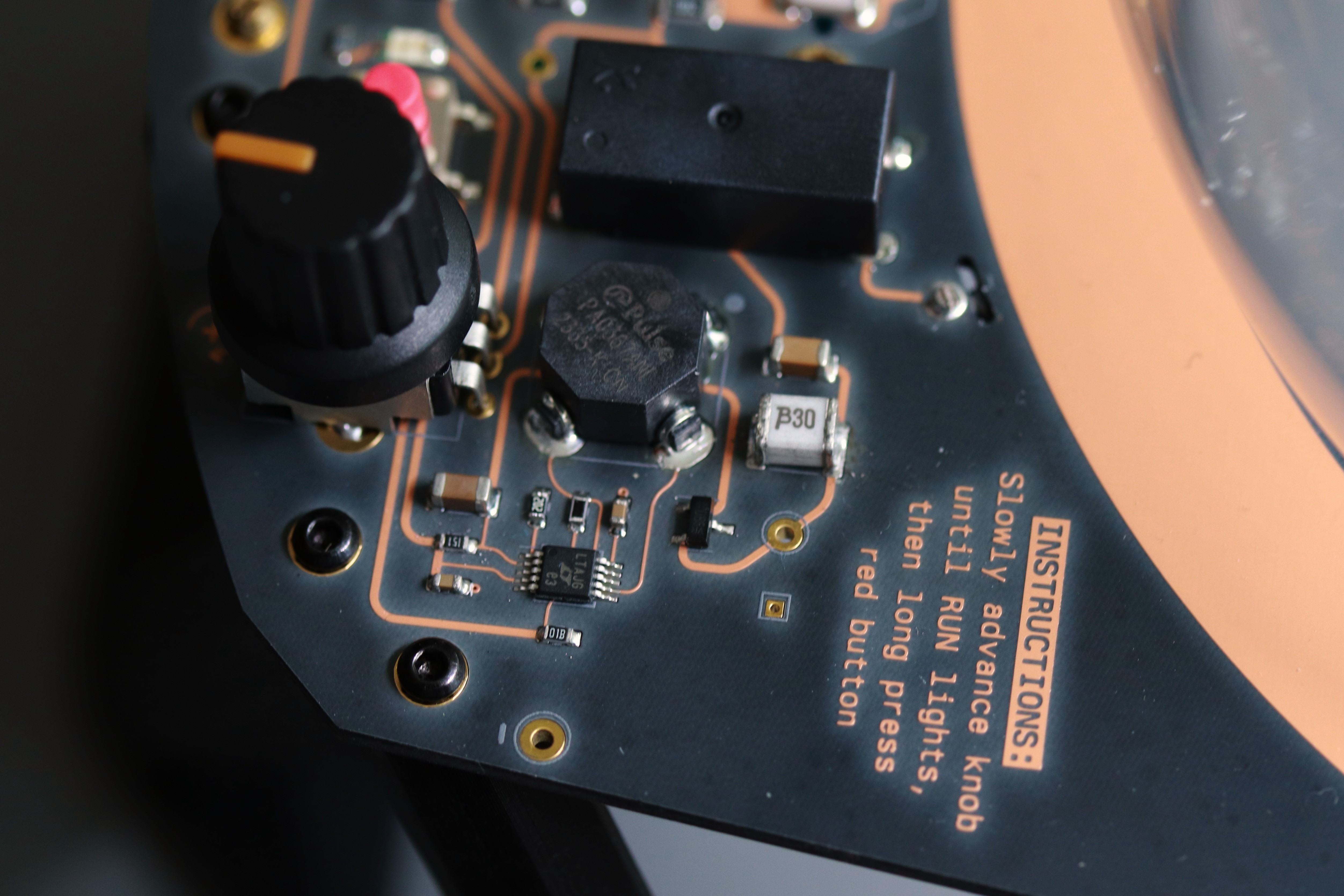
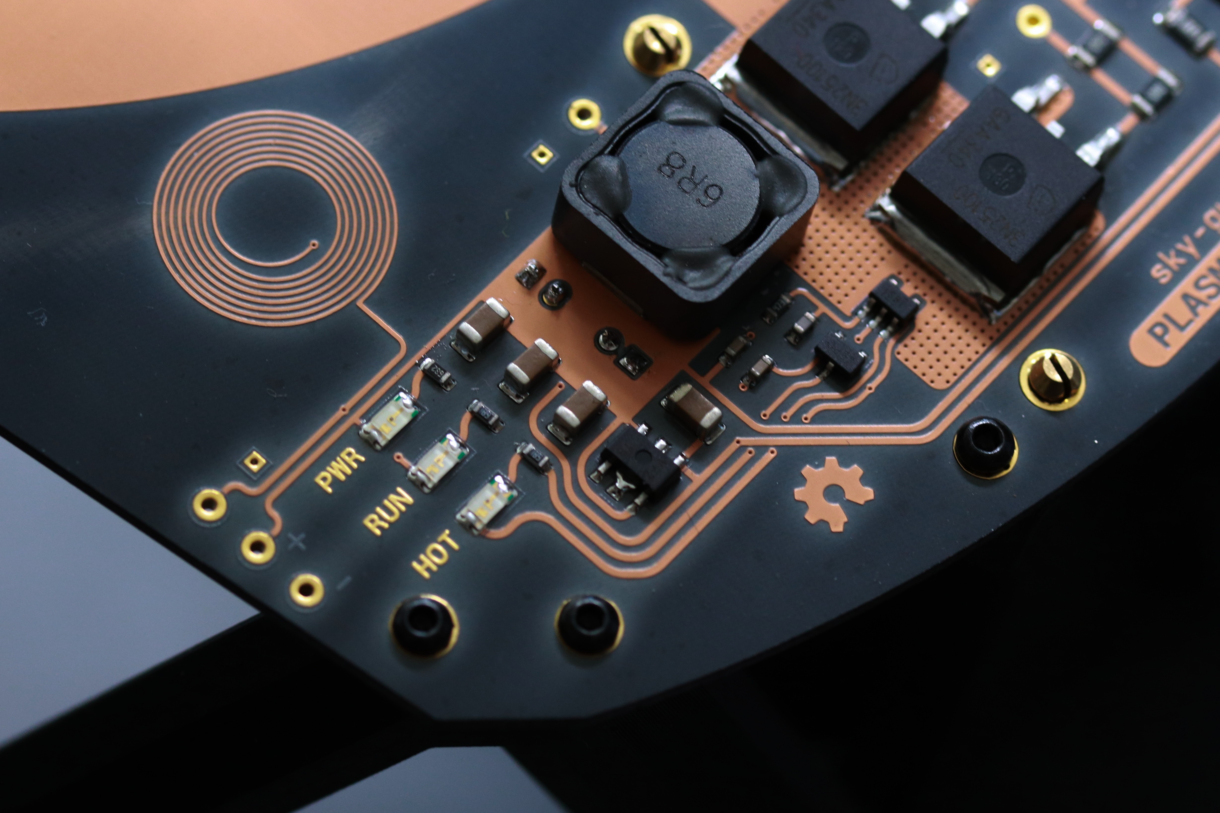
Typical PCBs use a olive-green fiberglass core, layers of copper, and a (traditionally green) soldermask layer to protect the copper and define areas where solder/component pads should stick. This board instead has a dyed-black fiberglass core and a transparent soldermask layer. This means that all traces are visible as their natural copper color, which is delightfully high-contrast against the black substrate. Component pads and other areas left uncovered by the transparent mask are plated (ENIG) gold.
This order of circuitboards was (partially) Sponsored by PCBWay! They covered about 60% of the cost of these boards, and I paid the remainder out-of-pocket.
There's very few photos out there of real PCBs made using this stackup, so I'm taking the time to write out a review.
(Transparency: being partially sponsored will likely bias my opinions, but I did also pay enough to feel like I have skin in the game. I have not given PCBWay any editorial control and they will not have seen this review prior to publication. Photos have been lightly post-processed and are broadly representative of how things look irl under good lighting. An order number [visible on the unpopulated board] has been blurred out for privacy.)
An in-depth look
This is going to be mostly photos.
Here's how the board looks straight out of the packaging
That looks really good, yeah??
The copper is a matte tan, not shiny at all. ENIG gold finish looks like it always does, and creates a neat kind of sandy two-tone.
For scale, the smallest traces on this board are 8mil with fairly generous spacing and the finest pitch component is 0.5mm. Components are D2PAK through 0603.
There's a sort of white ghostliness visible around the copper areas -- I'm guessing due to the transparent soldermask being not pressed quite as deep into the fiberglass. Under certain kinds of lighting, a faint weave texture of the fiberglass can be seen.
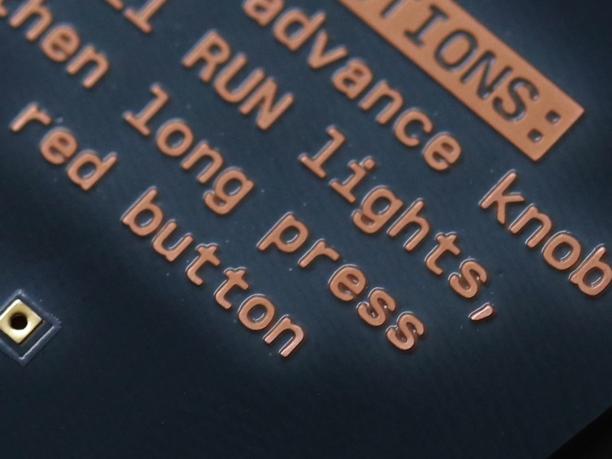
I absolutely love the way that text looks in copper. (This example has a character height of 1.2mm.) Super sharp! There's also a subtle dimensionality visible due to the thickness of the copper and the drape of the overlaying soldermask.
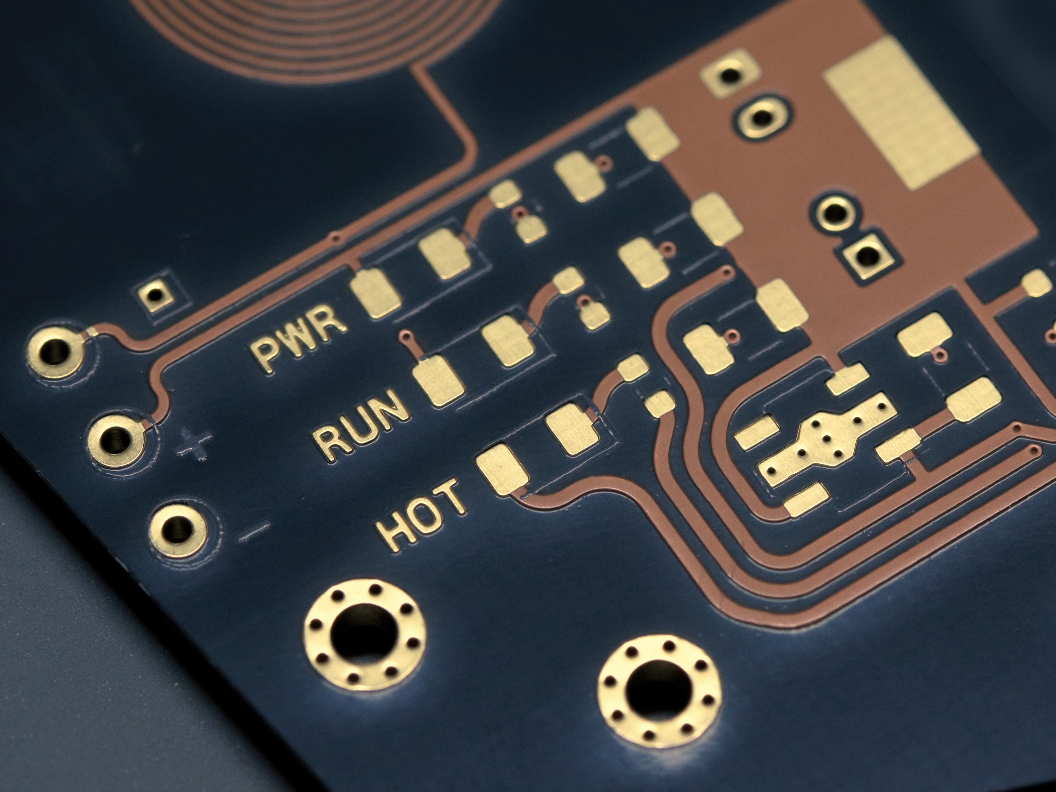
Text in copper+soldermask also looks nice and sharp (although is some slight cruft visible in the notches on the N and W). Contrast is more variable than copper-only as lighting changes, as the gold catches ambient light and reflection differently than the semi-gloss transparent mask.
The grey silkscreen ink is a bit mis-aligned from the other layers. This photo above shows it especially clearly: take a look at the holes on the left side and the silkscreen circles are distinctly off-axis. Silkscreen alignment has been better on my other PCBWay boards, which makes me wonder if the layer required some kind of hand-alignment that's less automated for their higher-order-volume stackups. Not an actual problem but definitely a bit unfortunate.
EDIT, ADDENDUM: My PCBWay sponsorship point-of-contact was perturbed by the soldermask alignment and raised it as a possible issue with their production team. In email correspondence with one of their customer service reps, PCBWay stated that while white silkscreen is aligned by machine, other colors (including grey) are aligned manually and "there will be +/-6mil offset which can not avoid. QC is based on the standard that the silkscreen are not on the pad."
Their Advanced PCB overview lists silkscreen offset as ±2mil, which is presumably representative of their alignment standards for white silkscreen.
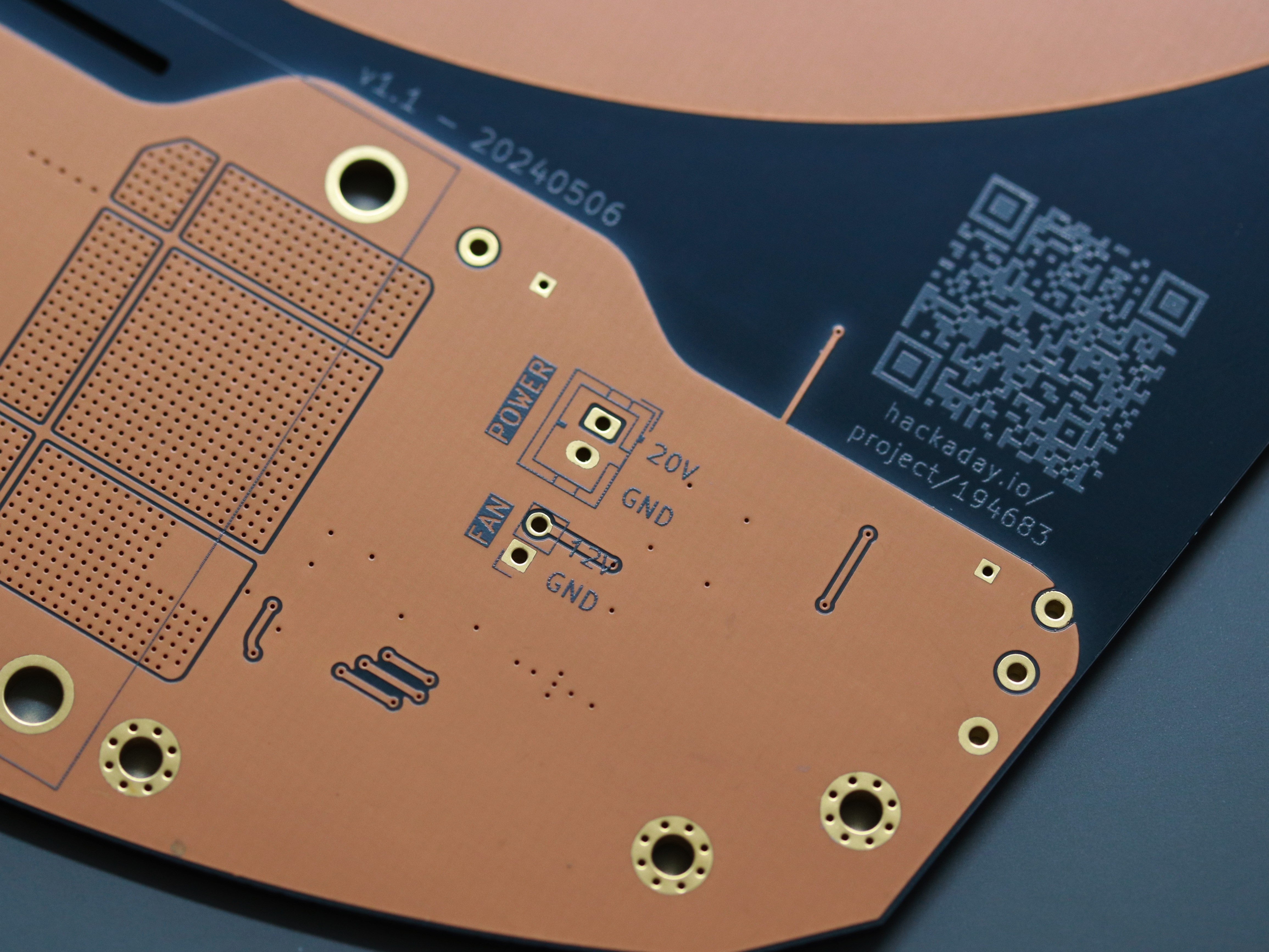
Here's the board backside with its large ground plane. They grey silkscreen QR code is plenty legible against the black FR4. (White silkscreen would be more typical against black, but I thought grey would be a bit more elegant and am happy I made that choice.) The bottom silkscreen is equally mis-aligned as the top.
Grey silkscreen over a copper fill is nice and high-contrast, but readability on the "12V" marking has suffered a lot where I placed text overlapping the edge of a trace.
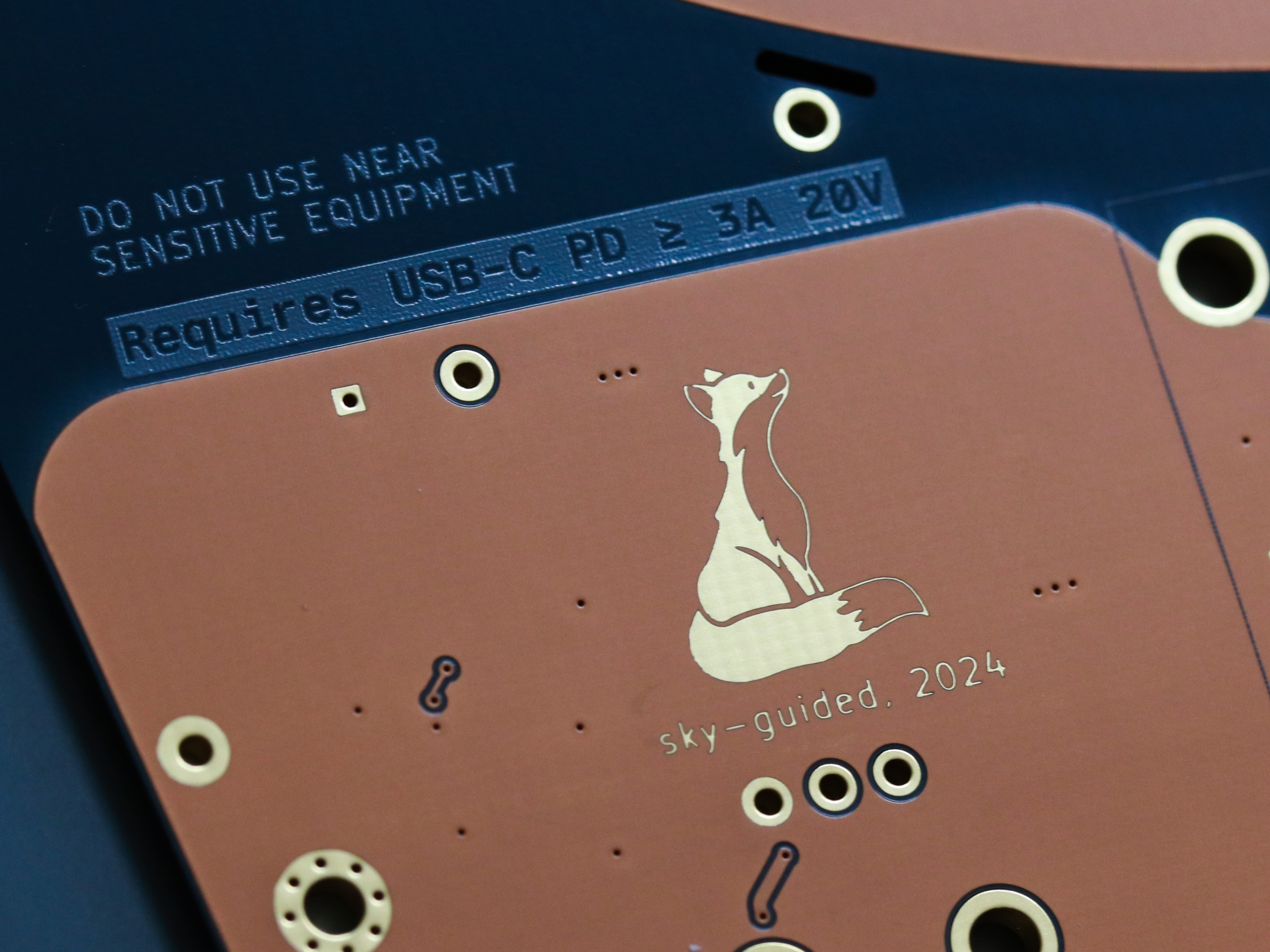
An art layer in soldermask on a copper plane also looks pretty good. The "sky-guided, 2024" text is 1mm high and 0.2mm stroke width -- I personally wouldn't go much smaller than that for soldermaskmask graphic strokes over copper. I didn't try gaps in mask over FR-4 because I didn't think it would be usefully contrasting.
Throughout this board, I used the KiCAD plugin "rounded traces" to make the traces curved and flowy rather than angular.
The Cost
Here's the catch though: this board stackup was much more expensive than a standard PCB.
Instead of the quick-turn "Standard" service, getting the black FR4 and transparent soldermask requires the "Advanced PCB" board fab. This run of five 190x145mm boards cost about nine times as much as if I'd purchased a normal stackup (not including the fixed costs of shipping).
As I mentioned up top, sponsorship covered a big chunk of that, but the sponsorship took the order from "nonviable" l;to "still quite expensive". Also as a note, the web order form under-estimated the cost until PCBWay Sales was able to review and give me a final quote. (Their sales team seems distinct from the representative I've been in contact with for sponsorship.)
I suspect that the cost differential would be a lot lower had I been ordering 50,000 boards (or maybe even just fifty) instead of a mere five. I don't have insight into what that pricing might look like.
I also don't know how the costs would change for a much smaller board area.
PCBWay sent a full test report for the board -- the "send me a test report" boxes on the order page were checked by default, and un-checking them didn't change the initial cost estimate so I figured why not.
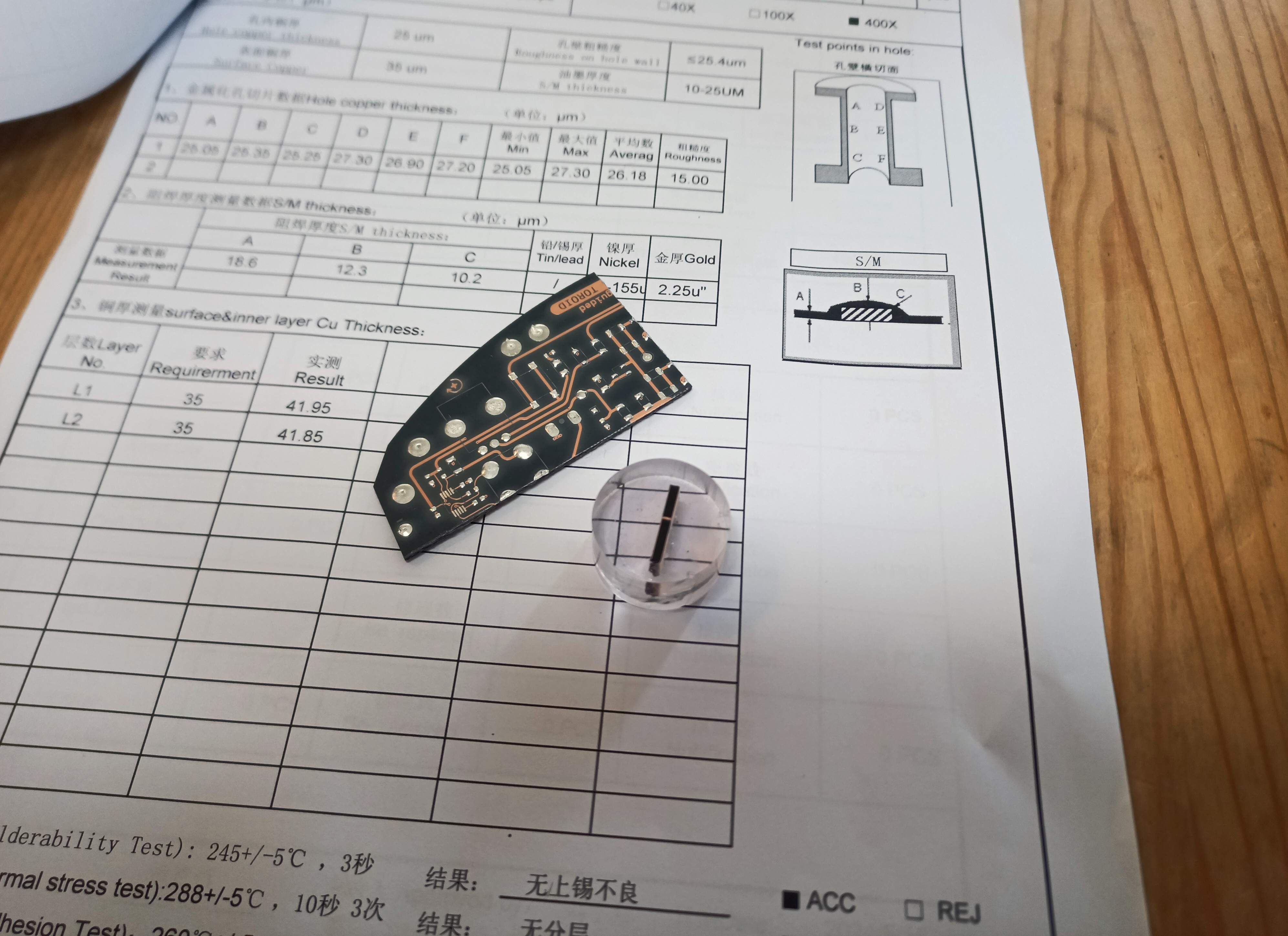
Here's just one page of the extensive test report, plus the two included section boards,one of which was a slice embedded in resin! Quite honestly I didn't need any of that testing -- this board isn't even high-speed enough to be impedance control. I think this is all standard practice for the "advanced" fab service.
Which all raises the very important question: as currently priced,
Who is this stackup meant for?
If I'm correct that the cost differential would be a lot less with a large-volume order, that suggests a commercial client might find this stackup a lot more worthwhile. However, I don't imagine there's not a lot of production-quantity products which would benefit from a highly ✨aesthetic✨ PCBs. Enthusiast computer motherboards, maybe? But in most cases, I doubt companies would want to pay even a modest premium for this kind of prettier board.
And on the other hand, I can see a lot of hobbyists who would be super-excited to have a project board (or limited-market production run) looking this swag, but for whom the high cost is totally prohibitive. I would be willing to pay maybe 3-4 times as much for this stackup in select projects, but not 9x as much.
Perhaps this kind of pricing would be fine for convention badge PCBs, which could make use of the unique look while also being both physically smaller and ordered in large enough quantity to offset setup cost.
The tooltip for the Black FR-4 option on the PCBWay order page suggests the opacity could be useful for some LED applications, but that seems a separate concern from buying black FR4 + transparent mask for visual appeal.
US-based PCB fabricator OSHpark also sells this stackup (under the delightful name "OSHpark After Dark"), but their per-square-inch pricing model would have made a board as large as mine even more expensive. They're also slower. If your board is a lot smaller, you might consider them as an option.
Final Thoughts
I absolutely love the way this board looks, and I'm glad I'm able to use it for my project.
I also wish it were more accessible for other hobbyists. My hope is that PCBWay could figure out a way to get this stackup out of the super-bespoke Advanced PCB production pipeline, since a lot of that functionality is completely tangential to "pcb looks really neat". My suspicion is right now there's the catch-22 of it's too expensive for folks to order, and lack of orders makes it stay an expensive specialty product. Perhaps some kind of special promotion could break the deadlock?
I should also emphasize, these thoughts on pricing are based on the pretty limited sample of this specific large, prototype-quantity board. If that pricing is wildly anomalous, then these hot takes are probably off-base.
To wrap things up, here's one more photo:
Being hyper-conscious of "I want to make this board look exceptionally good" did make laying out and routing the PCB take much longer than it would have otherwise.
I'm happy I took the time to do so. It does look exceptionally good!
Coming in the next update: project showcase, wrap-up, source files, and thoughts for anyone looking to make a toroid of their own.
Discussions
Become a Hackaday.io Member
Create an account to leave a comment. Already have an account? Log In.
This is sick looking!
Are you sure? yes | no