 cziter15
Be careful when considering ground pours on outer layers, as they are typically unnecessary for 4+ layer PCB stacks.
✅ After further research, I removed the ground pour from the top layer. It wasn’t needed and could introduce issues if not implemented properly. However, if you really need to ground pour the outer layers, ensure proper via stitching to preserve signal integrity.
✅ I also updated the module's firmware, enabling it to operate at a 115k UART speed, which significantly improved its stability and responsiveness.
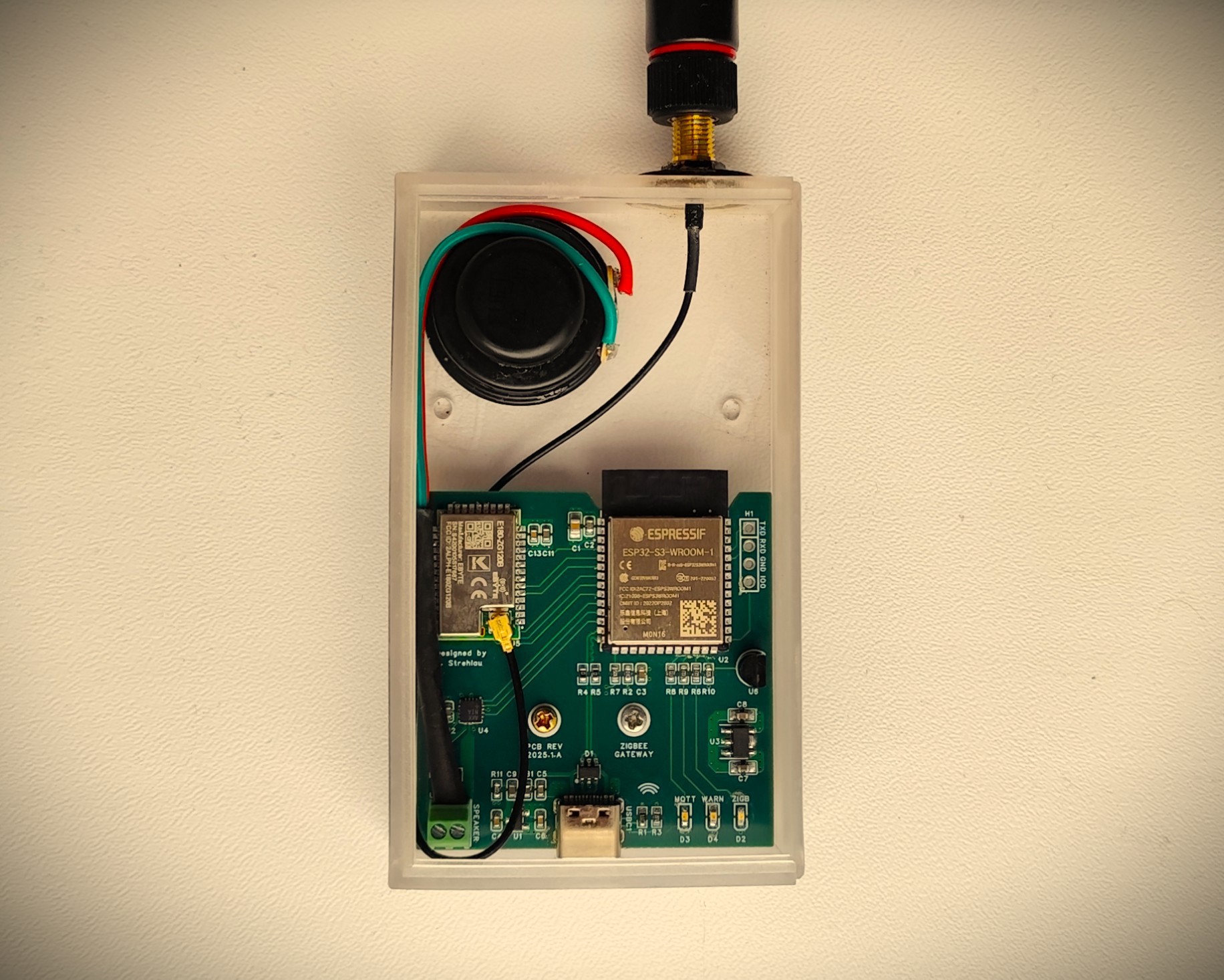
✅ I have migrated to the new PCB, and now all my smart home devices are operating as they were before.
Discussions
Become a Hackaday.io Member
Create an account to leave a comment. Already have an account? Log In.