 Bud Bennett
There has been a lot of DIY effort to make a good, cheap constant current electronic load. I must give homage to the efforts of past attempts, mostly successful, to create something useful for evaluating a power supply's capability or a battery's capacity. It's not easy.
One of the best is Dominik's: https://github.com/Dominik-Workshop/Electronic_load/tree/master
His implementation covers most of the bases and we used it as a benchmark. But it is a bit lacking in user stupidity protection. (And we wanted more.)
Another implementer worth mentioning (besides our eminent Hackaday colleagues) is John Sculley with his excellent treatise on YouTube: https://www.youtube.com/playlist?list=PLUMG8JNssPPzbr4LydbTcBrhoPlemu5Dt
But alas, Mr. Sculley descends into the mire of fixing unforeseen predicaments in a seemingly never-ending fix-it scenario. I guess a nice way of putting it is "Feature Creep".
We recommend viewing Kerry Wong's excellent YouTube videos (https://www.youtube.com/watch?v=WUPrj03UbTM) on Linear MOSFETs for an education in the reality of "Safe Area of Operation", or SOA, for the uninitiated.
This is a Team Effort:
Paul has been working on this for a while. I entered the scene when he had a problem with oscillation that he couldn't explain while evaluating his latest prototype. Paul's blog on this subject is here: https://www.paulvdiyblogs.net/2024/09/building-diy-dynamic-dc-load.html
He covers the build process in a lot more detail and has the Gerber files and BOM, along with a supplemental BOM for specialty parts and their sources. What you find here is just the circuit design aspects.
Project Status (2024-12-02):
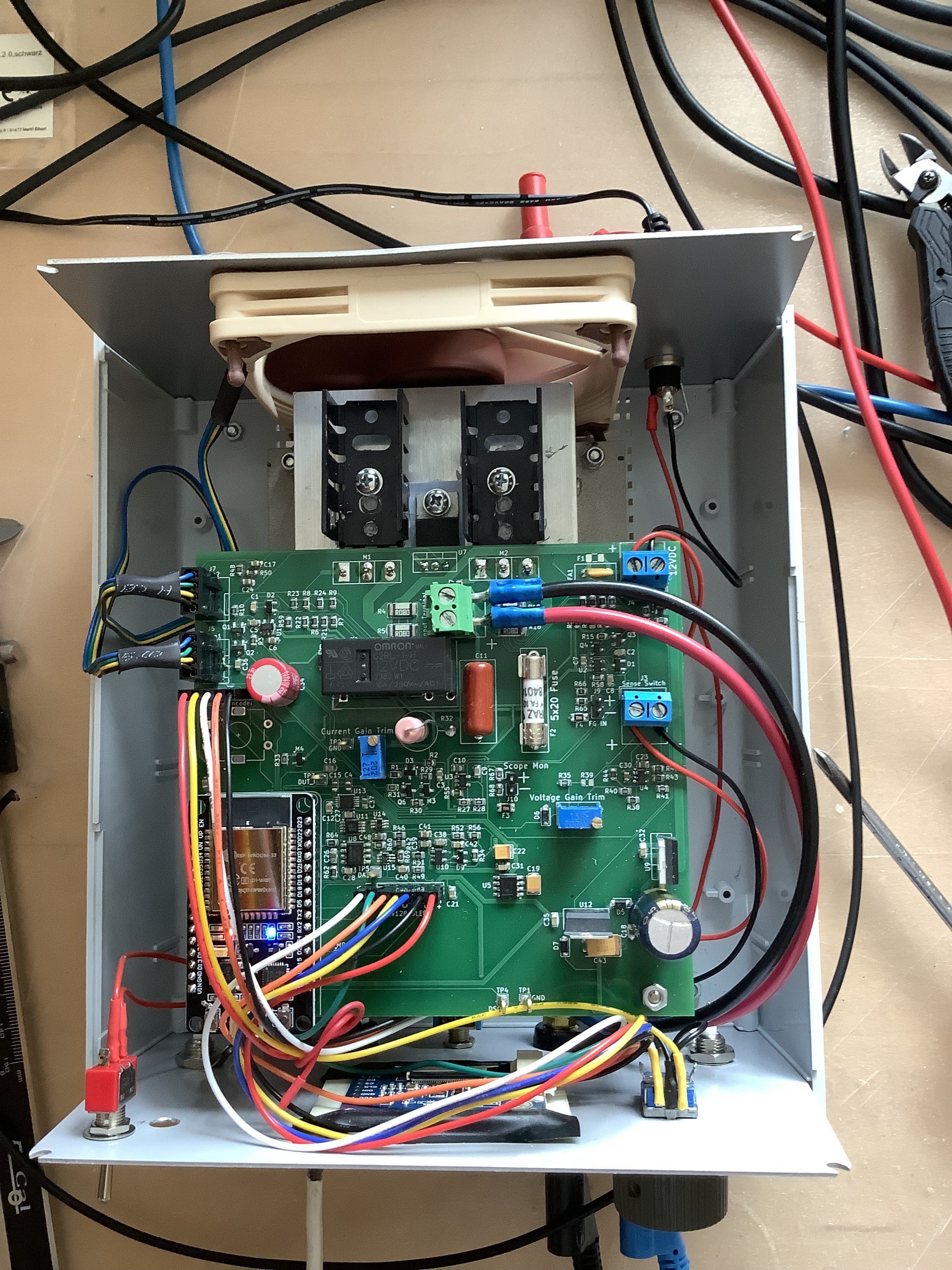
The PCB (rev 5.1a) is the our final version, which fixed the problem with second fan not running.
There are now two fans for thermal management. The two fans are wired in parallel -- there are two 4-pin fan connectors on the PCB. One fan, 92mm, sits below the heat sink and blows cool air up into the fins. The other 92mm fan is mounted at the rear of the enclosure and suck hot air out of the enclosure. This has been tested to 185W, the limit of my power supplies.
The enclosure is another problem. It should be plastic, to isolate the heatsink (which is connected to the output terminal) from the user. Paul found an acceptable enclosure -- a Teko AUS 33.5 (198x178x108mm) -- but it is not readily available in the USA and the shipping is costly. Paul is going to create PCB panels for the front and back to make it look less DIY, so this is the only enclosure we recommend that you can purchase (though there is an option to print your own, or have somebody else print it). This is what the inside of the enclosure looks like with the current PCB revision:
Target Specs:
Input Voltage: 1V - 100VDC
Input Current: 1mA - 4A for 40V < Vin < 100V, 1mA - 10A for 1V < Vin < 40V.
Maximum Power Dissipation: 150-200W (Depends upon heatsink and Fan.)
Voltage Accuracy: 0.4% (Trimmed, but there are temperature drift terms.)
Current Accuracy: 0.4% (Trimmed. Mostly temp drift error.)
Lowest Conductance: Untested. (Current NFETs + Sense R + Relay contact R = 75mR)
Ripple: Untested.
Protection: Reverse polarity to -100V. 15A fast blow fuse at input.
Power Input: 12VDC/1A Wall Adapter. Reverse polarity protected to -24V.
Cost: $200 (Aproximate. $35 Case, $38 Fans, $23 OLED, $12 Heat Sink, $6 ESP32, ~$75 Assembled PCB, $10 Misc Hardware.)
User Interface:
Display: 128x128 Color OLED.
User Input: Rotary Encoder with push switch. Remote/Local voltage sensing switch on front panel.
The Software:
Pretty much done at this point (rev 26b). See Paul's Github page to download files.
The Hardware
Here is our final schematic (as of 2024-06-10).
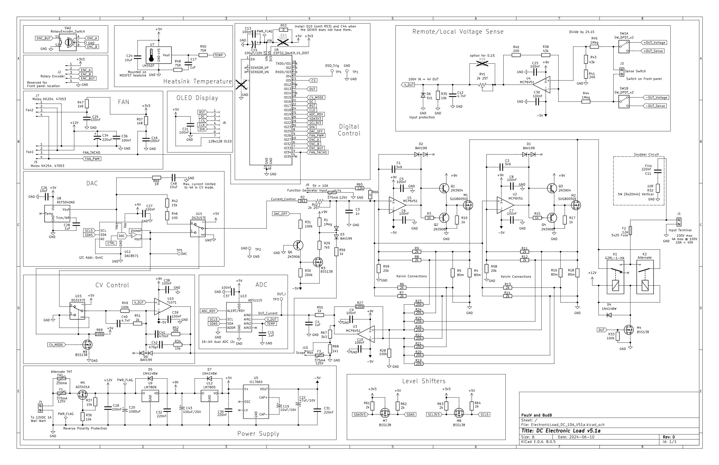
The first thing to notice is that there is a relay and fuse to protect the circuit guts against inadvertent stupidity. It's better to replace a fuse than toss an entire circuit in the trash. The nice things about relays are that they don't leak current when they're open and have decent contact resistance when closed. The system will power up with the relay open and it will be open with the power off, so if the user connects the load with reverse polarity it can be sensed, a warning issued and the the relay kept open until the reversed connection is removed. There are two relays to choose from: an expensive one ($20 --Paul's) and a cheap one ($1.5 -- Bud's). Unfortunately the two relays don't have the same PCB footprint.
The voltage and current feedback are from instrumentation amplifiers that are calibrated with a trim for accuracy. The current feedback amplifier's offset errors can be removed at system boot by measuring the zero current feedback voltage and subtracting it. The voltage feedback amplifier is a zero-drift chopper-stabilized opamp that should have very low offsets. This still leaves temperature drift as an error.
The current resolution is set by a 16-bit DAC with a range of 0-4.096V. Its reference is the REF5040. The DAC output is divided down to a full scale 0.2048V to the current loops controlling the current through two 40mR resistances, so the full scale current is 0.2048/0.02 = 10.24A, with a resolution of 0.15625mA/bit. It will take 64 DAC steps to make a 10mA step. Paul gets to do the math.
The voltage/current feedback resolution is set by a 16-bit ADC. The ADC has an internal voltage reference = 4.096V. Voltage resolution will be around 1.5mV/bit.
The CV mode is implemented in hardware. The maximum current while in CV mode is set in hardware to 4A, but you can change it if you're brave. That way we can repurpose the DAC to control the output voltage setting. The resolution of the voltage control in CV mode is 16-bits -- 1.5mV/bit.
There are level shifters to compensate for the logic level differences between the ESP32 (3V3) and the ADC/DACs (5V) using the I2C bus.
We added a Function generator input (5V = 10A) to produce arbitrary waveforms. We also added a Current Monitoring capability -- a voltage output scaled to 1V = 10A, to see real-time current output on a scope.
Internal Power Supplies
We're using +9V, +5V and -5V for supplies. The ESP32 Devkit provides its own +3V3 as a source for logic level pullups. We would have preferred a +10V instead of the +9V, but the LM7810 doesn't have the headroom to do that. The opamps require +9V and -5V to drive the big NFETs. We needed the -5V to get to zero even with rail-rail opamps.
The -5V is generated from the +5V supply by a noisy ICL7660.
PCB Layout
This is what the latest PCB looks like:
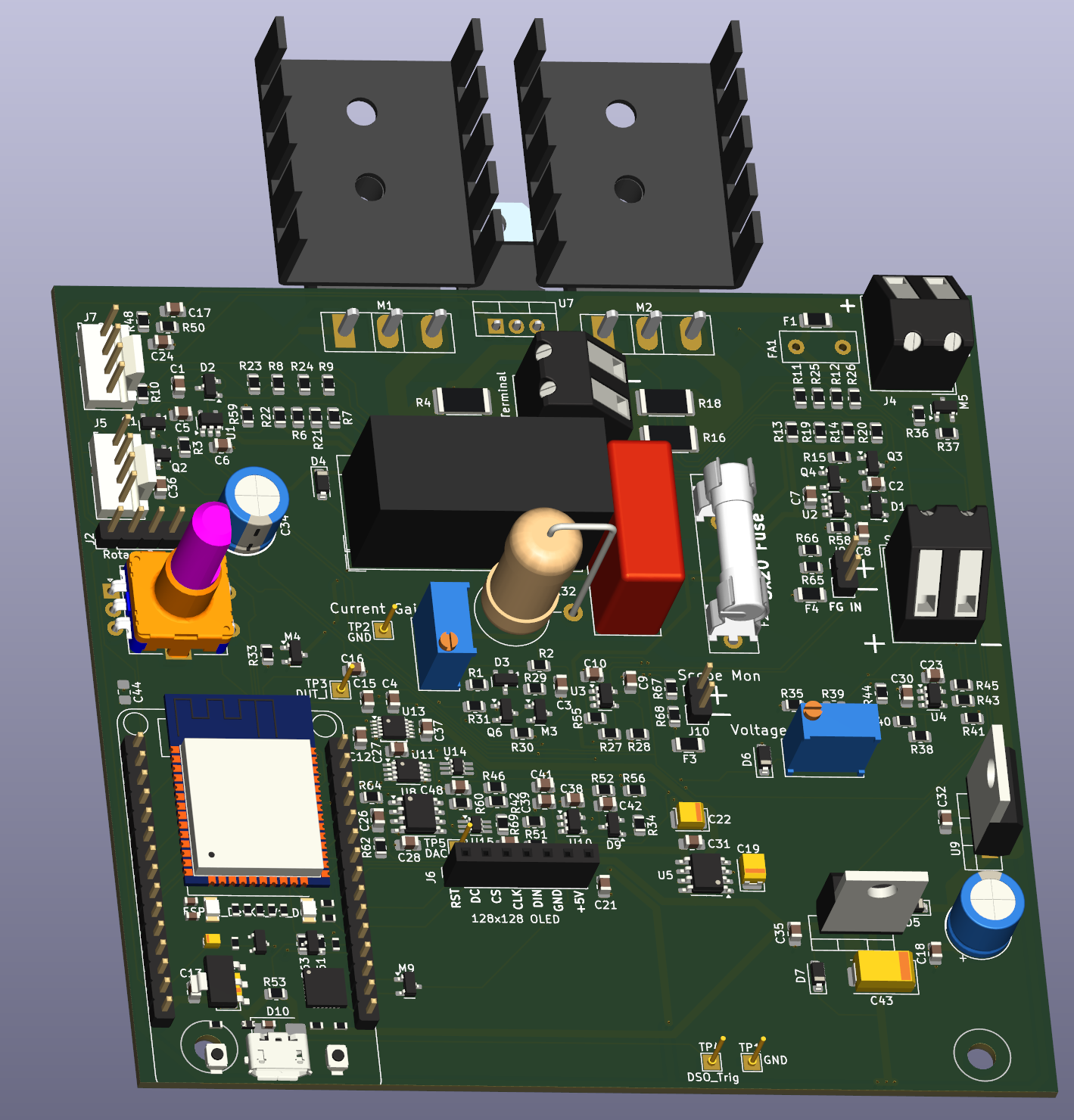
The previous PCB design had a tab at the top to mount J4 -- this was a byproduct of the particular heat sink that Paul was using. Since that heat sink is no longer available we removed the tab, which makes the PCB a nice rectangle now.
The encoder is mounted on the PCB only during development, otherwise in has a separate connector, J2, to connect it from the front panel.
The aluminum heat sink will sit below the PCB and the NFETs and temp sensor will be bolted to its flat surface. The NFETs and temp sensor have their leads bent at a right angle and are mounted below the PCB. The U-shaped TO220-type heat sinks are bolted to the tops of the two NFETs to help decrease the temperature rise. It decreases the maximum temperature of the NFETs by 10C, according to Paul. Yes, it looks funny, but they are cheap and if they work then so much the better.
It is easier to connect the input terminals to the input terminal block now that the NFETs are laying flat and the heat sink is below the PCB.