So next step was to make CAD design and CNC print. The result was amazing compared to previous methods. (Standard 3018 with CNC shield nothing fancy)
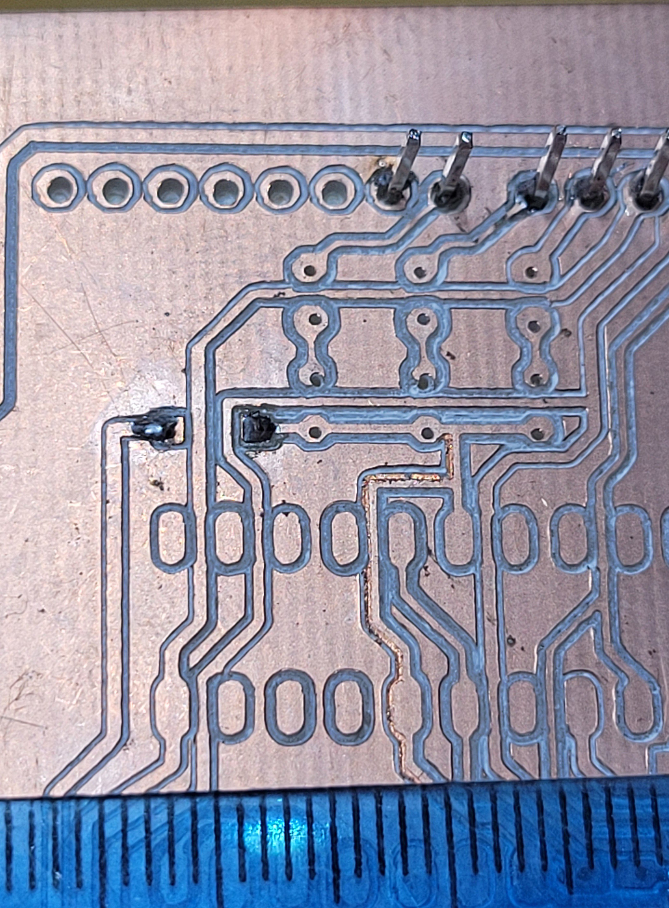
This how I reached about one mm resolution. It gave me ability to easy connect complex components. Boards could be manufactured in matter of minutes with many ICs on them.
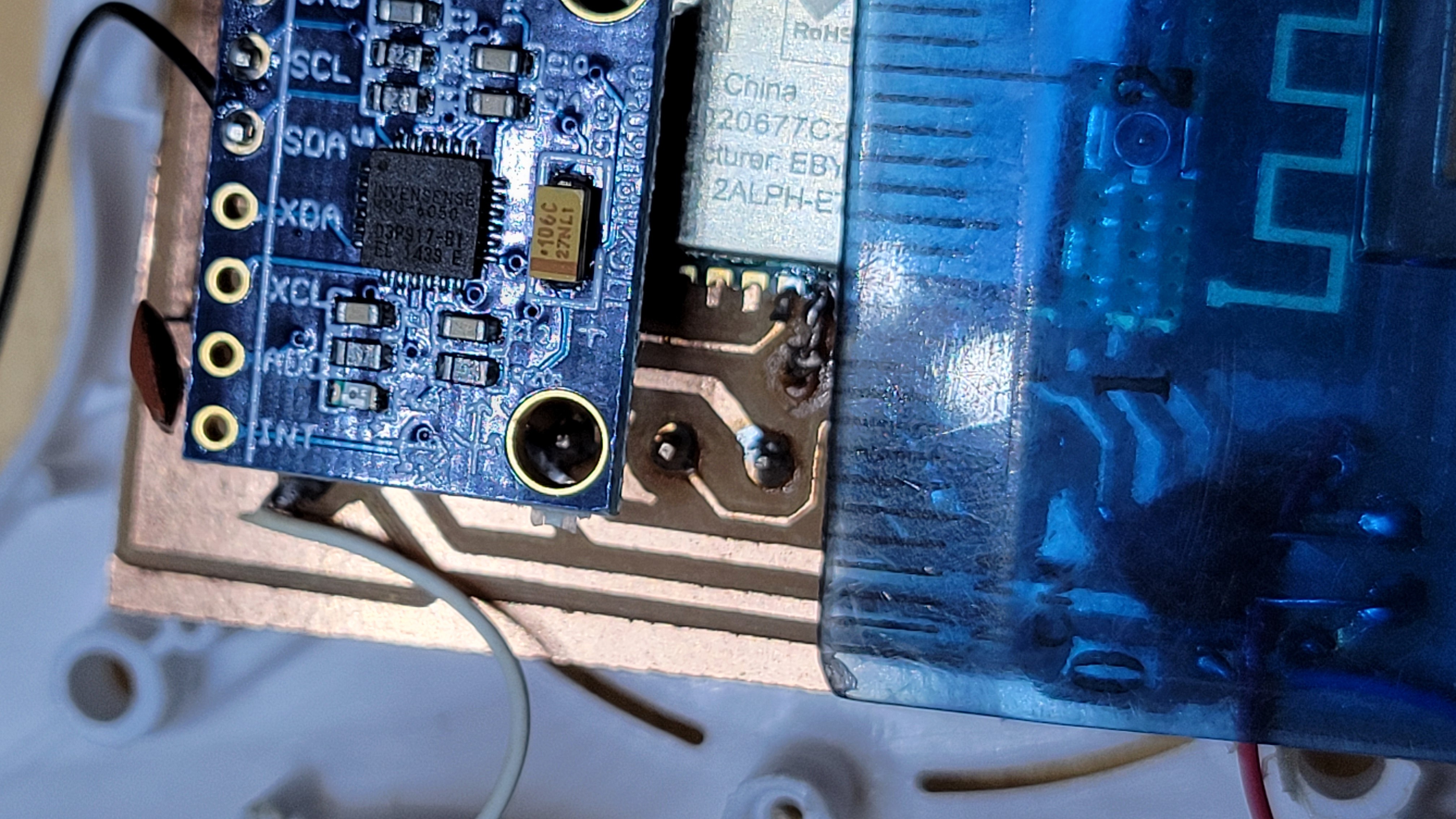
For example here I've connected MCU and gyro board.
Soon I hit a limitation, SOIC - Small Outline Integrated Circuit. Some projects used this tiny enclosure so tiny the width between terminals is only 0.5mm.
Smaller detail usually could not survive. After a lot of try and error I found that it's possible
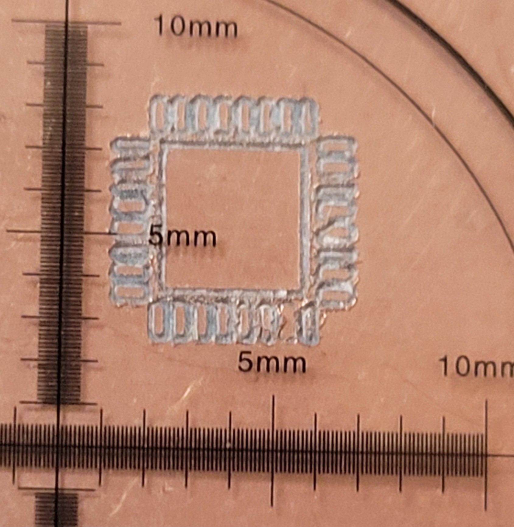
But the problem remained why some print were successful and others failed.
To understand that let's look on the problem from microscopic point of view.
Discussions
Become a Hackaday.io Member
Create an account to leave a comment. Already have an account? Log In.