 kelvinA
I've been working on the brushless motor PCB for the past 4 days. I'm starting to write this log when its not completely finished (I've still got the power nets to connect and the UWV pads to place), but it's to a point where I can say that a 14 x 15mm controller PCB is probably possible:
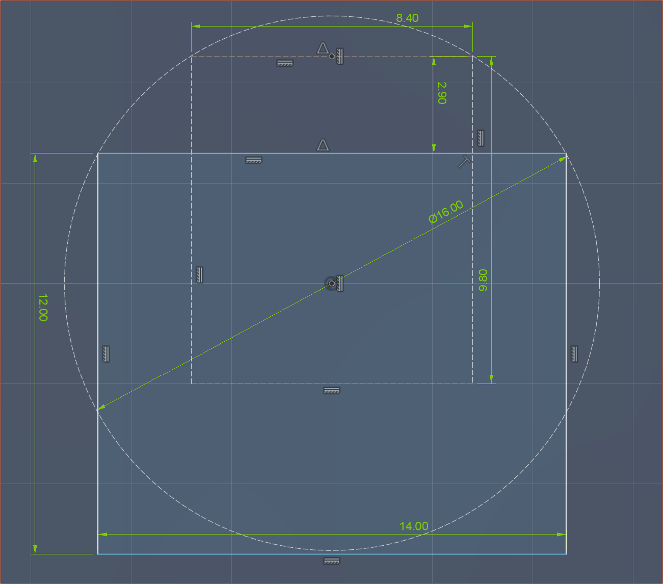
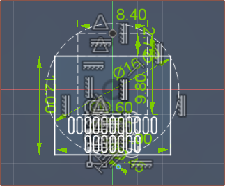
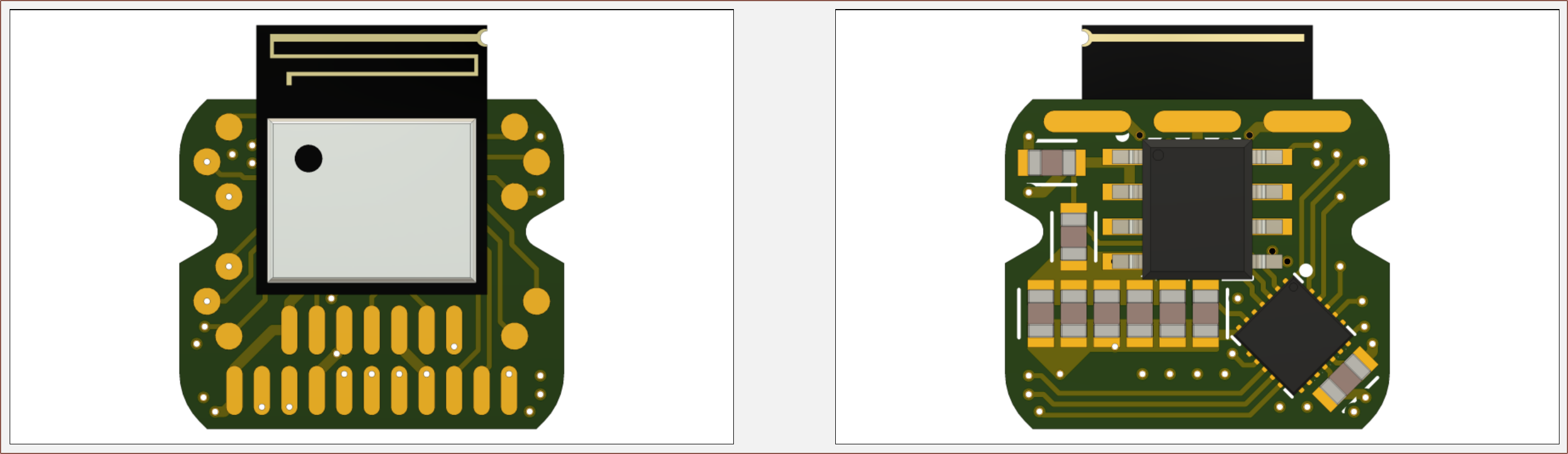
Planning the PCB size and placement
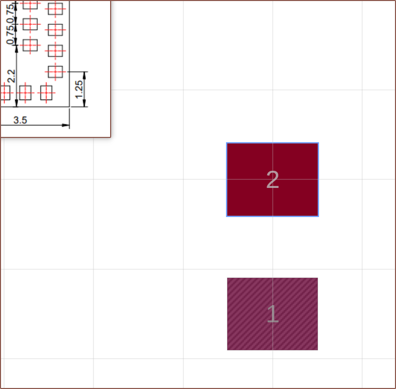
My expectation since the start of June was that I was going to have the 11 pin connector on the left and the 7 pin on the right, with test pads in the lower right. The 11 pin FCC should be 12mm, so that's what I set the height as. Additionally, I was thinking that the microphone was just going to complicate matters with waterproofing so I decided against it.
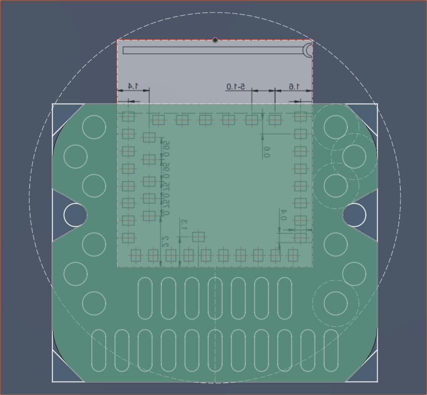
However, when I drew the dimensions of the MS51SF1, I saw 2 things:
- The edges of the PCBs are on the 16mm curve of the motor, conveniently enough
- There is a lot more space between the bottom of the module and the bottom of the board, potentially meaning that I could have both FFCs (flexible flat cables) coming out from the bottom (similar to the placement of wires on other BLDC motors).
The 2nd point was even more important as the motor and gearbox bearings go edge-to-edge, meaning that the FFCs would stick out.
I zoomed out till the PCB was 1 : 1 scale and decided to reduce the height of the pads from 2mm to 1.8mm.
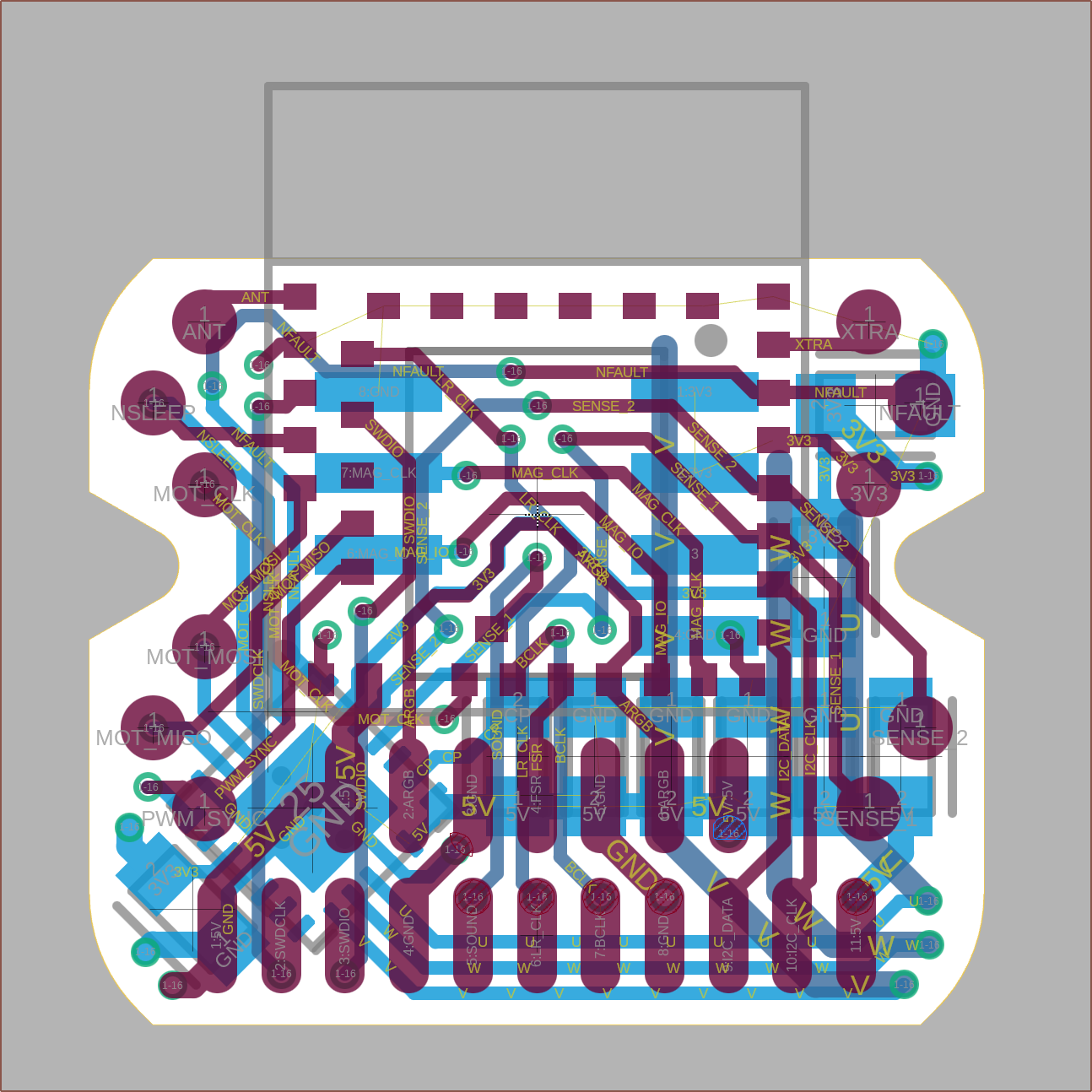
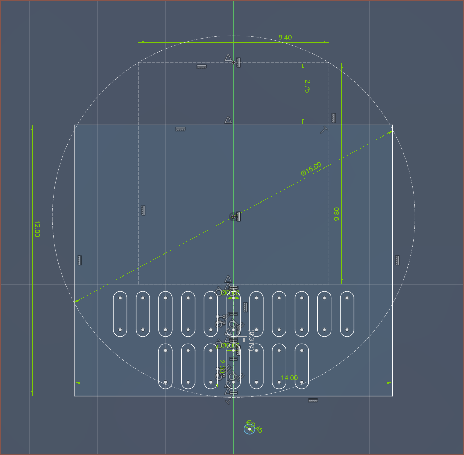
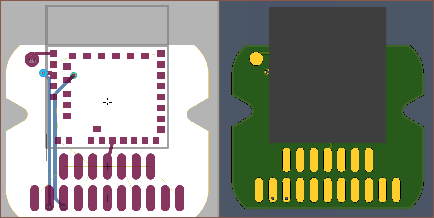
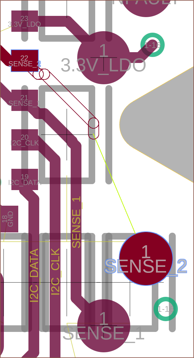
Then I had a think about how these cables were actually going to route out, and if the 7P was on the bottom, it would only be able to terminate on the other side of the motor. If I put it on the top, I could terminate on either side. It also had other benefits, like the FSR pin being neighbours to an analog input pin, or being able to fit a testpad array:
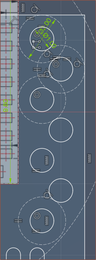
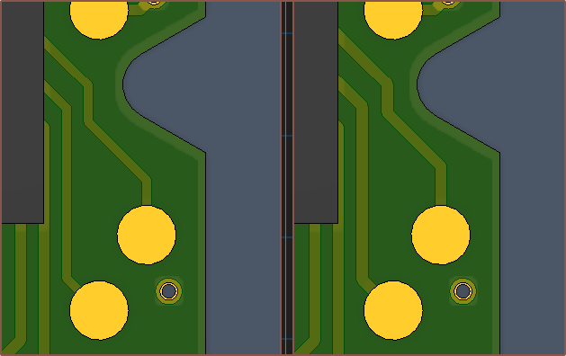
There also needs to be a mechanical way of keeping the PCB in place, so I converted the 4th-pad location into a 60 degree V cutout:
Creating the MS51SF1 schematic component
So I drew all the pins and labelled them, but then scrolled down in the nRF52833 and found out that there are 3 different packages for it and they each have different pins that are slow or are recommended for the SPI clock. I looked in the SF1 schematic and deduced that they were using the WLCSP variant, which has a lot more "low frequency I/O" pins than the aQFN I was initially looking at.
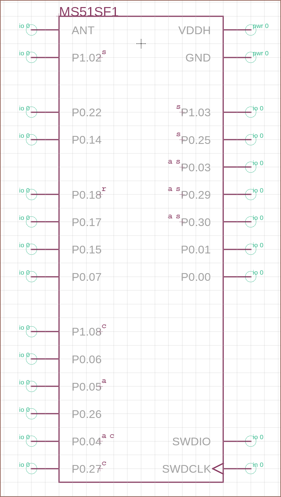
I'm hoping I don't actually need that reset pin. I don't think I do:
Then I started the tedious process of placing pads. It didn't take long to see how KiCAD did things, but it doesn't look like grass is greener on that side. It's just a lot of addition and data entry to get the pads in the right places, and the reason why I decided to keep everything in the positive-quadrant instead of trying to make a footprint centered around the origin.
After making the footprint with the correct pad numbers, I duplicated it and deleted the pins I knew I wasn't going to use (USB and VDD):
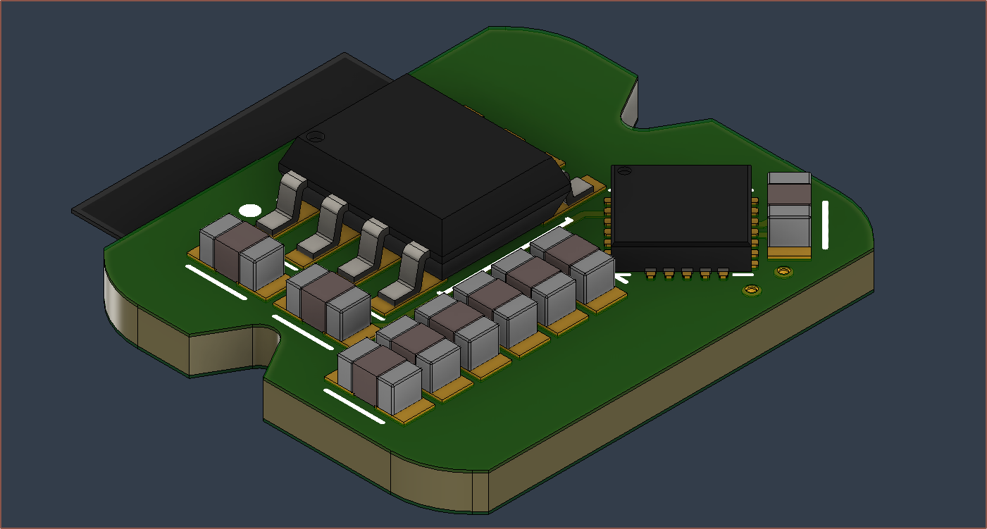
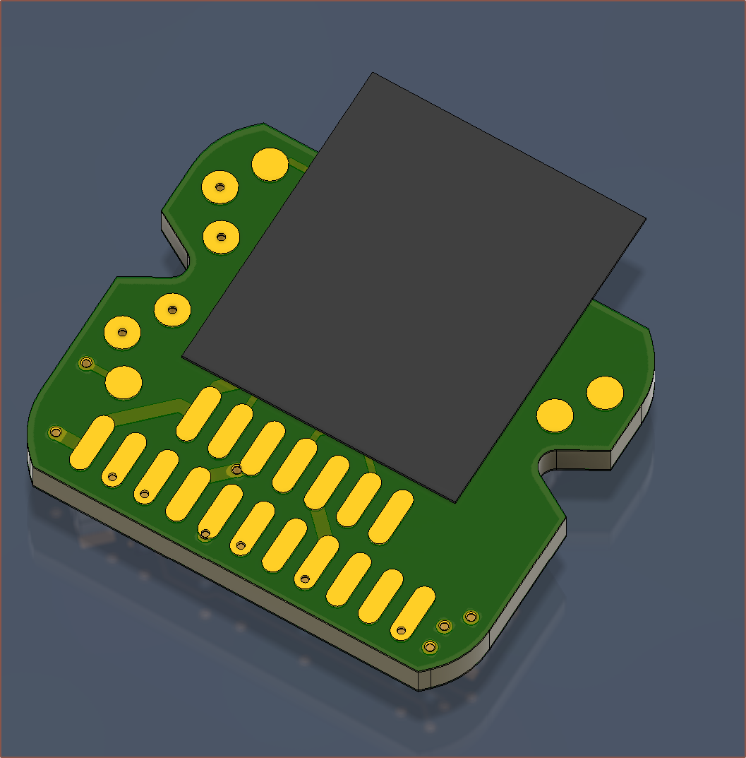
Then I placed some starter gear on the board to confirm everything actually works like how it was planned:
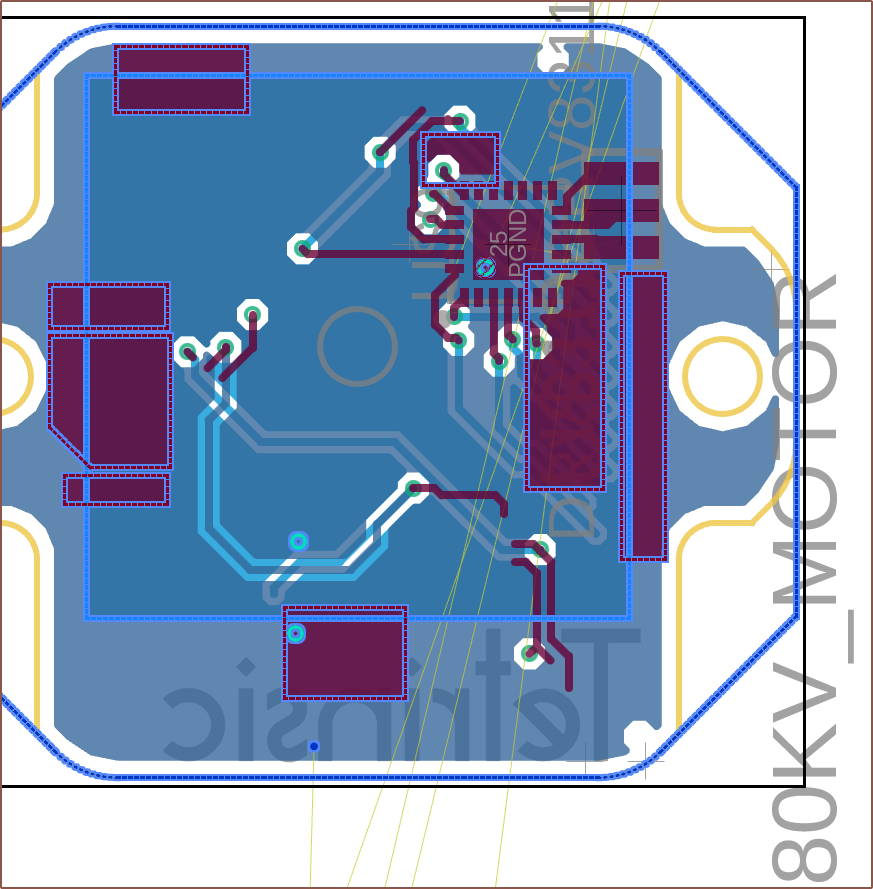
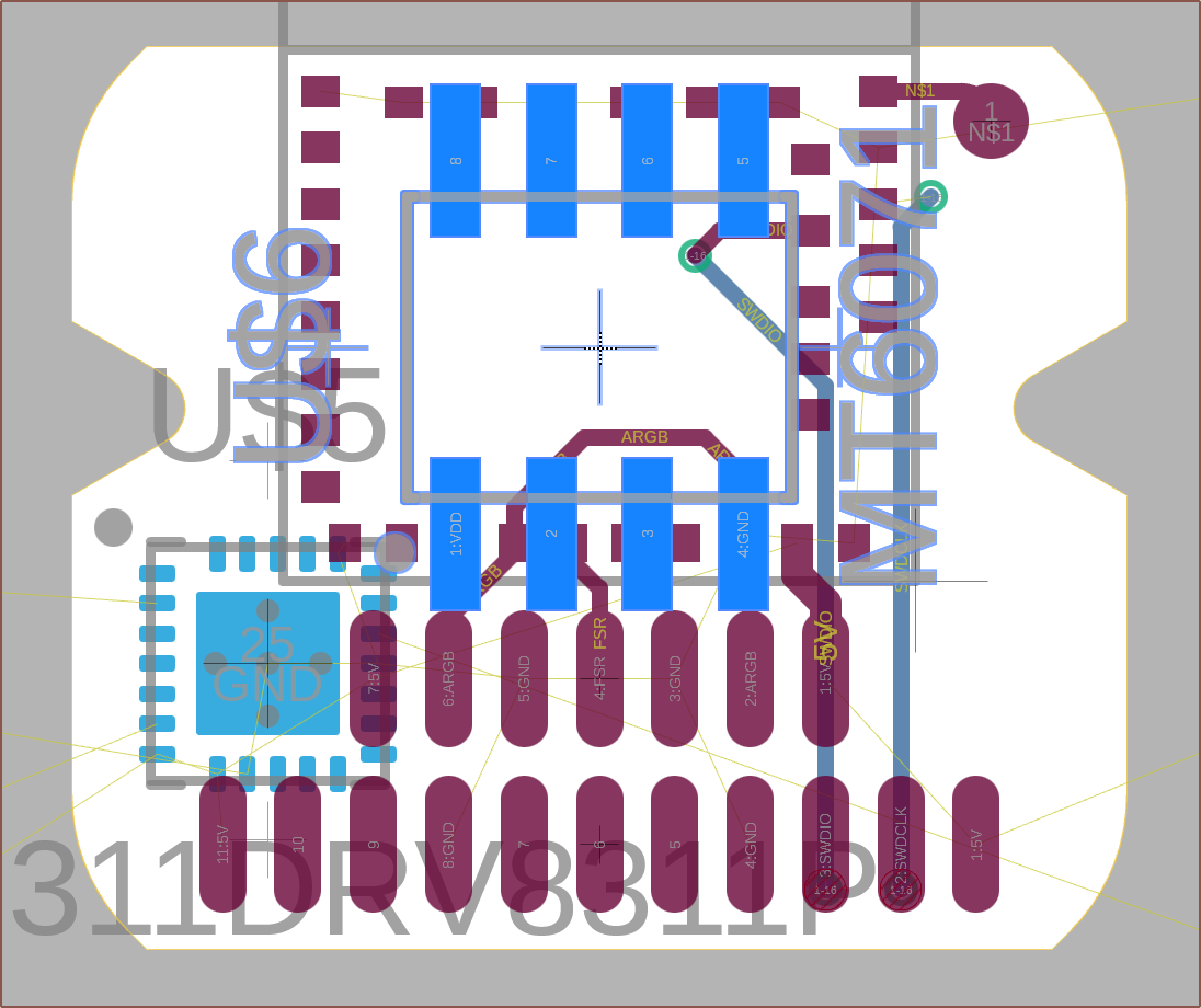
The DRV8311P (BLDC controller) and MT6701 (magnet sensor)
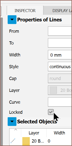
For some reason, I can't just copy part of the old schematic and place it in the new one, so I had to "Insert Electronic Design" and then delete the other parts of the schematic. This also imports the PCB apparently:
I had to first unlock the lines before I could delete them:
Additionally, I still felt like the 8SOP version of the MT6701 would be better than the smaller 16-QFN because the pins would be more spaced out.
 So then I had to move the DRV and it's bundled passives around to find a solution which I could tap out. After exhausting the search space for 90 degree options, I looked into diagonal placement and that's when a solution existed. The magnet sensor also needs a capacitor and an optional protection diode.
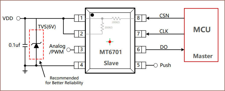
 Continued routing and was having space issues, and then I noticed that I wasn't using pin 5 on the 6701 for anything (it's the PUSH output) so I removed the pad:
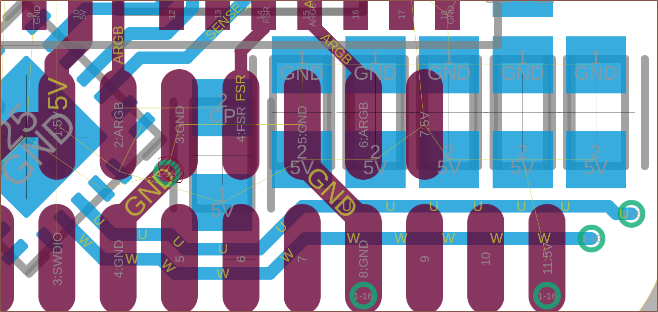
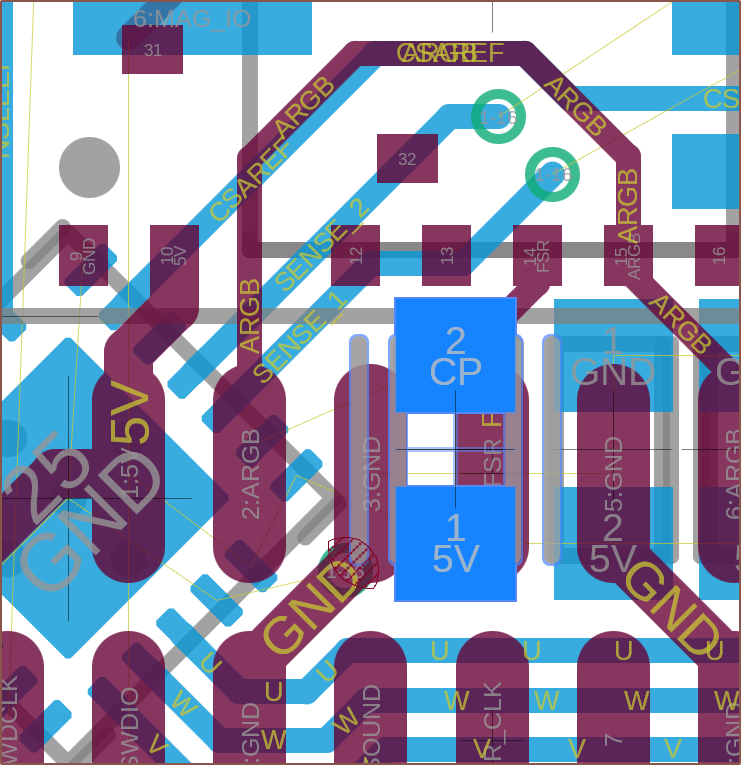
Something that I didn't see when I made the first PCB was that the CSAREF pin actually needs a reference voltage source and read by the ADC:
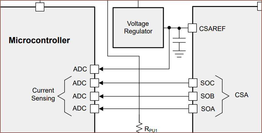
I decided to connect it the the 3.3V LDO, as well as the 6701 since its IO logic levels are derived from it:
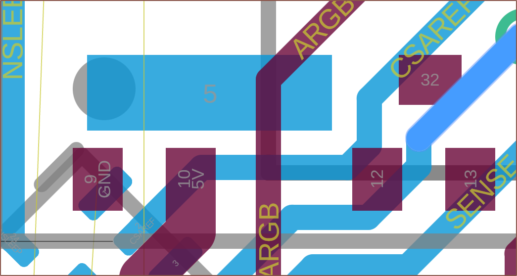
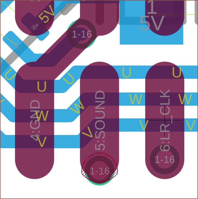
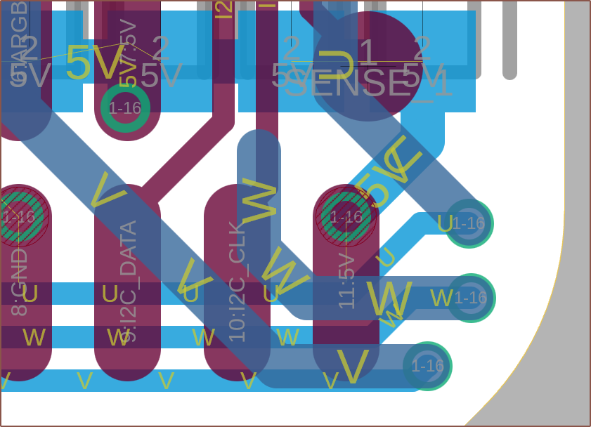
Routing pads
Next Steps and Conclusion
- Design UWV pad
- Connect airwires
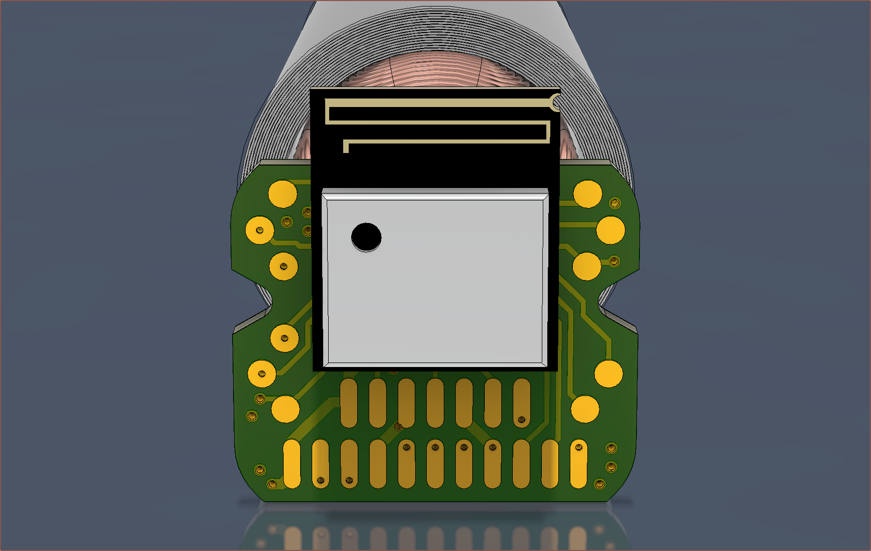

Fully traced and copper pours added
- moving the silkscreen dot of the MT6701 off the UWV pad
- spacing the CP capacitor from the 5V ones to prevent shorts during manufacture
- replacing one of the 100nF 3.3V capacitors with a 5.1K pullup for nFault (recommended in datasheet)
- It made little sense that two bypass capacitors were so close together, which would likely change the frequencies filtered out.
- changing LR_CLK to use P0.18 as I found out that its frequency is dependent on the sound sampling frequency (e.g. 44.1kHz).
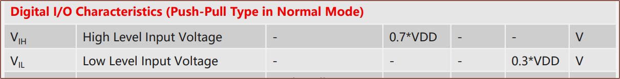
- I looked into it, and the "low frequency I/O" note for the nRF52 is actually a caution for the radio, not the pin in question. From what I understand, the pins with the note are very close to the radio circuitry and frequencies higher than 10kHz could diminish performance of the radio. The GPIO will work completely fine.
- P0.18 is configurable as RESET, so I likely will need to configure "softreset" when flashing firmware.
Discussions
Become a Hackaday.io Member
Create an account to leave a comment. Already have an account? Log In.