 Keith
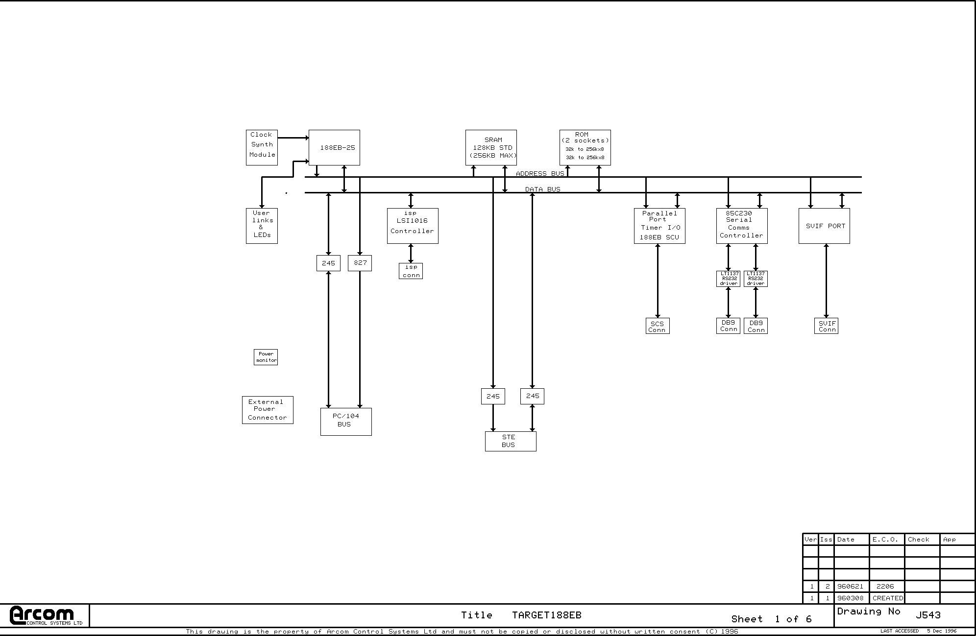
Keith1a. Block diagram
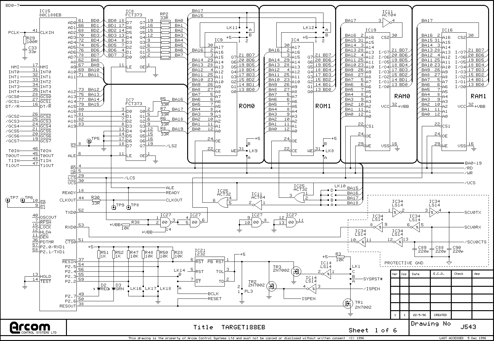
1b. CPU and memory
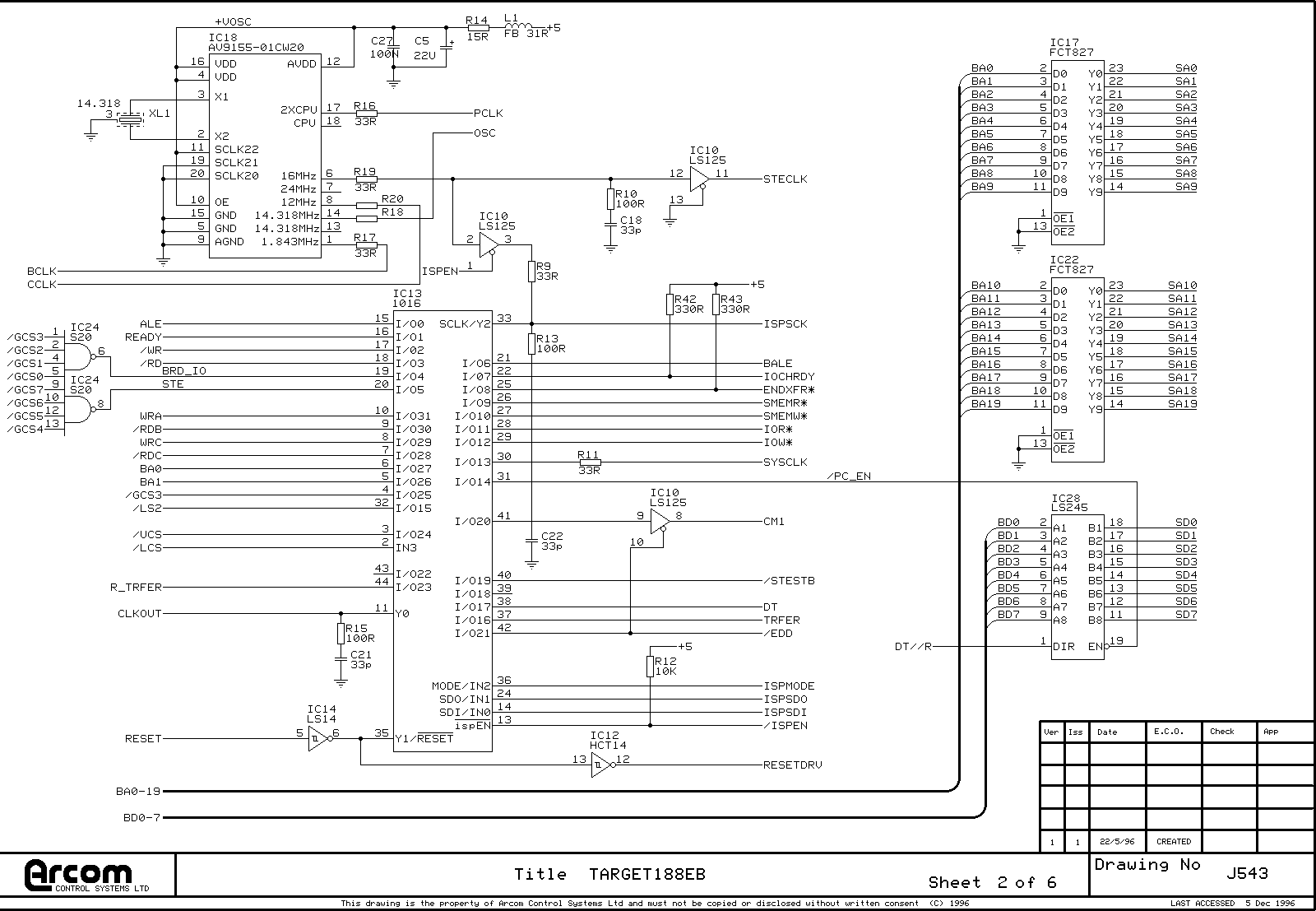
2. Clock and glue logic
3. Serial I/O
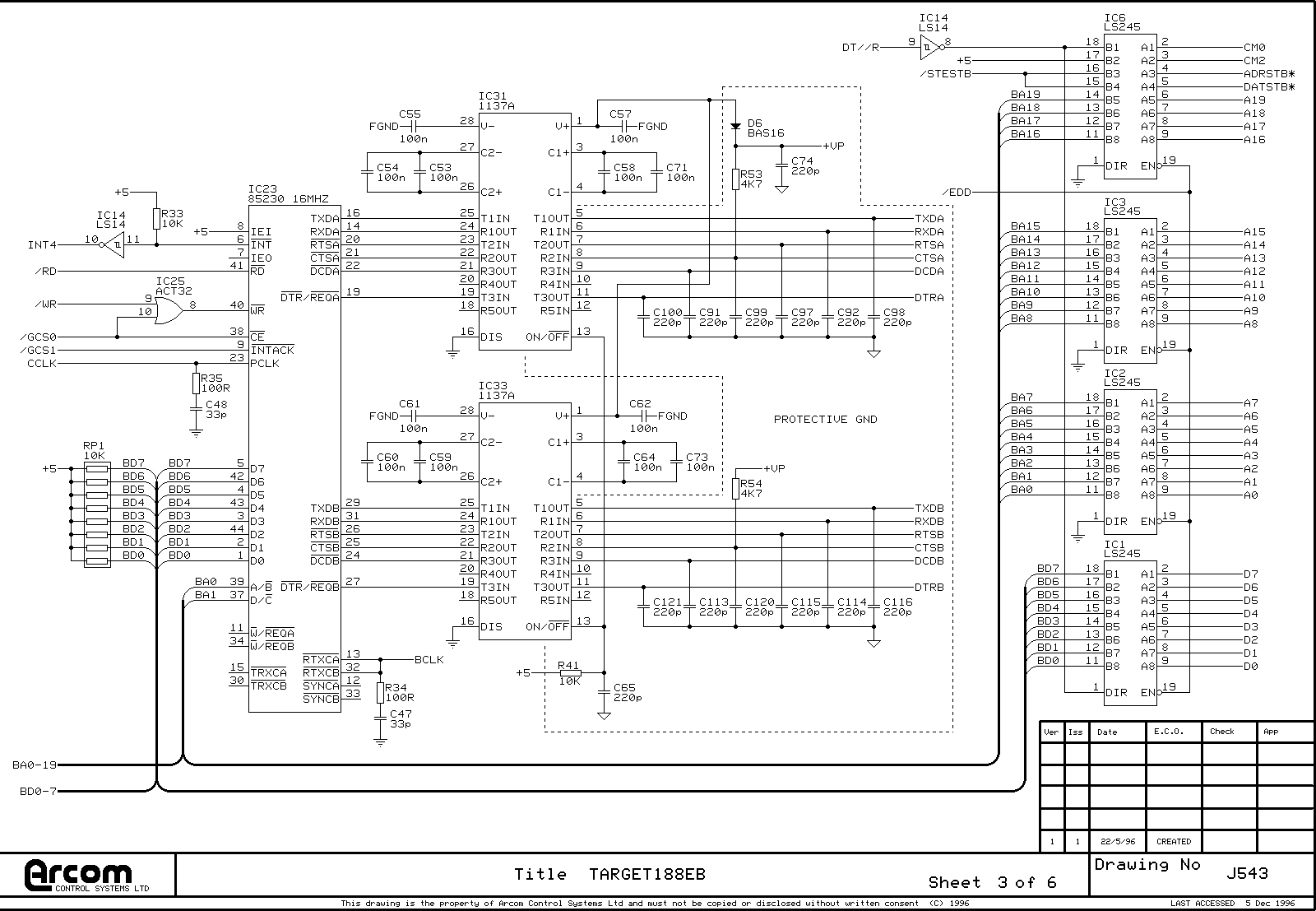
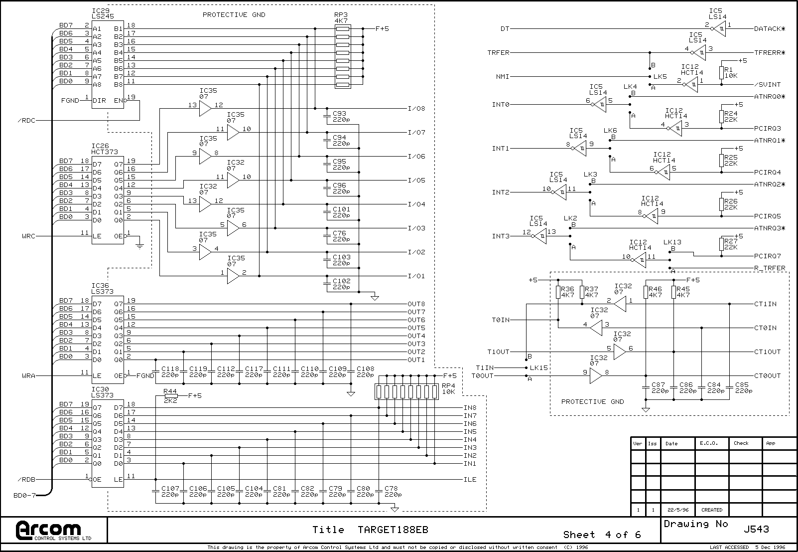
4. Parallel I/O
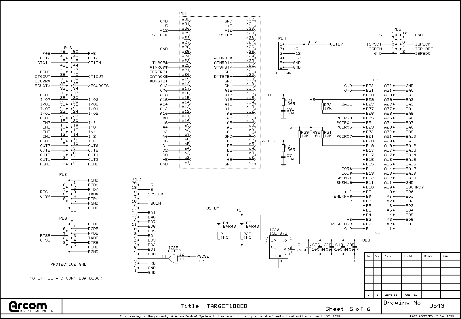
5. Bus connections
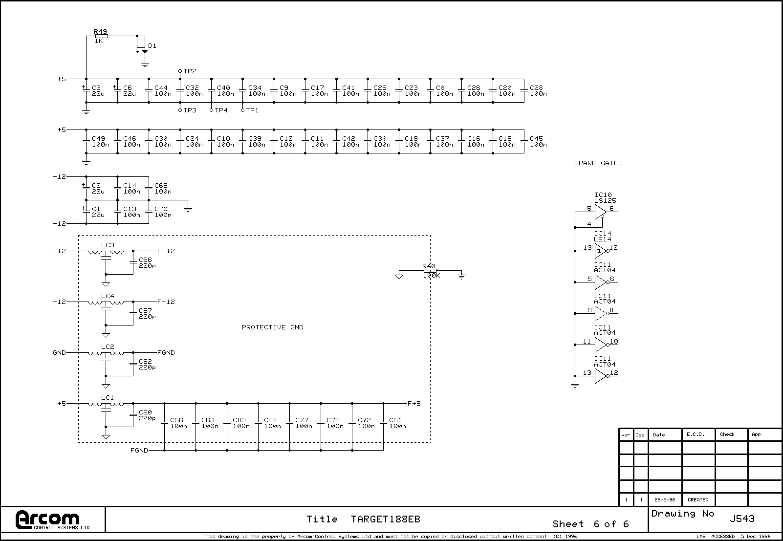
6. Decoupling and spare gates
A project log for STEbus and PC104 bus 80188 CPU board
A master of two popular industrial buses
1a. Block diagram
1b. CPU and memory
Discussions
Become a Hackaday.io Member
Create an account to leave a comment. Already have an account? Log In.