 Clyne
ClyneHere it is! The boards came out great:
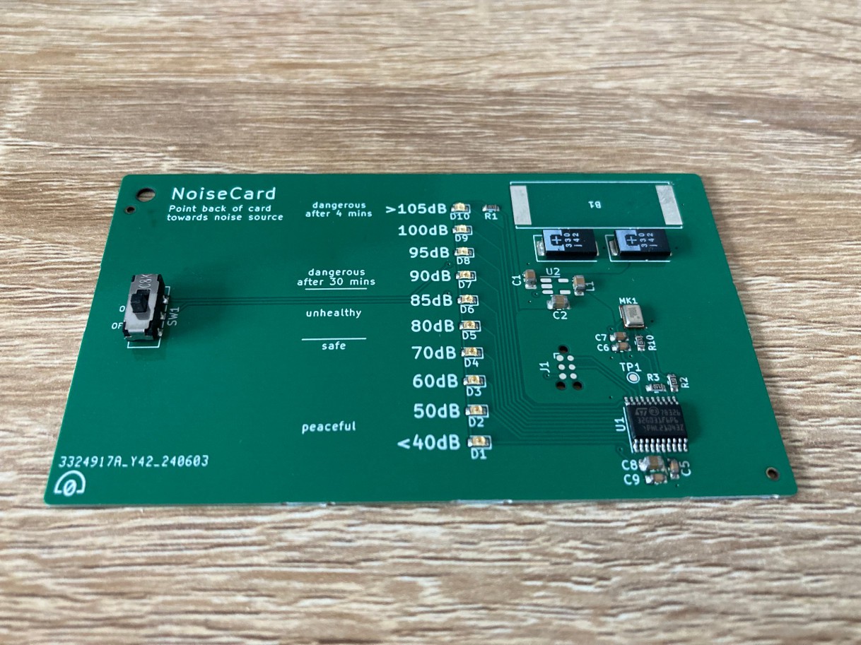
Only one issue with this batch: L1, the inductor for the switching regulator, got a capacitor placed on its footprint (see it above near the unplaced U2). I apparently overlooked this when JLCPCB generated a BOM for me. Fortunately, I was able to pull a substitute off of some other boards.
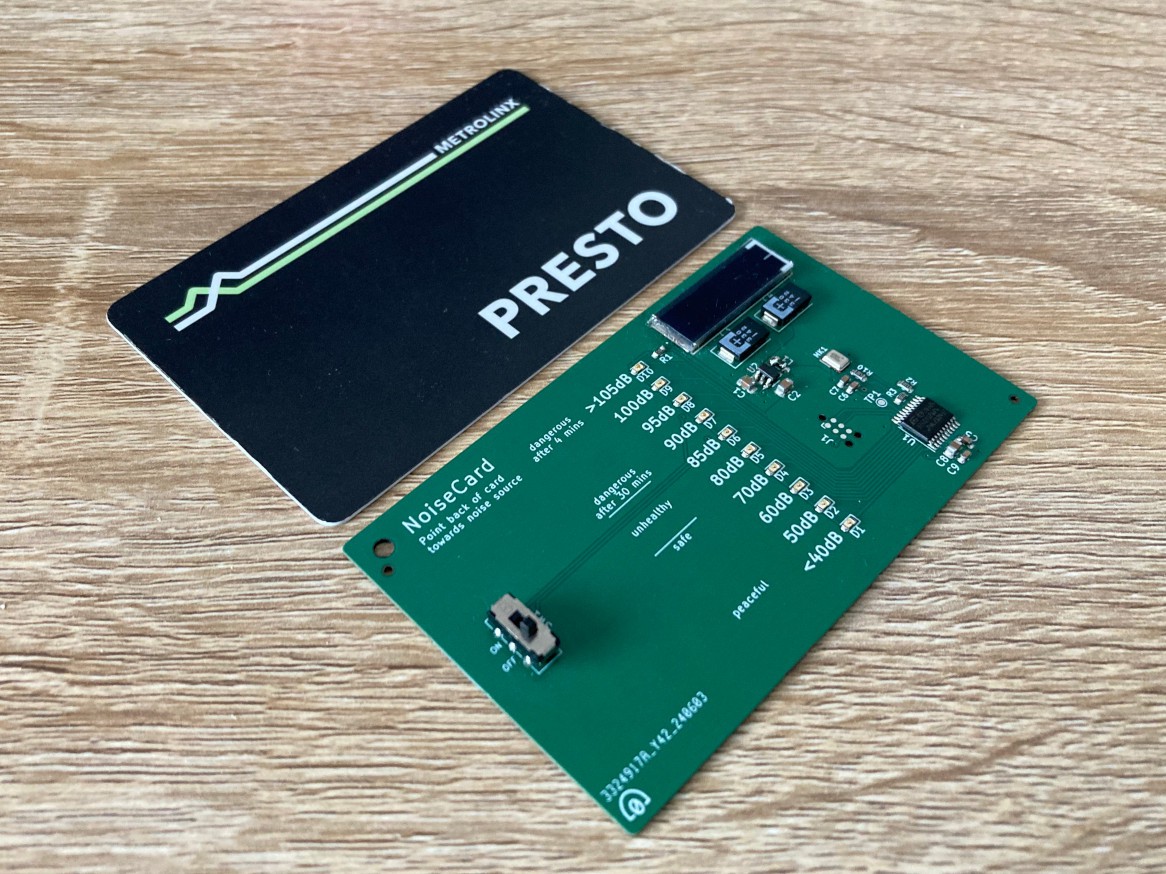
Here's a fully assembled board below with a regular card for comparison. The solar cell was a pain to solder on, with barely any room to heat solder between its underside pads and the PCB footprint. I tried a heat gun, but that started to melt the cell's coating before heating the solder below. For now, I just loaded solder onto the pads so I could heat it with my iron while squishing the cell down. In the future, I'd consider using through-hole pads that I can just fill up with solder.
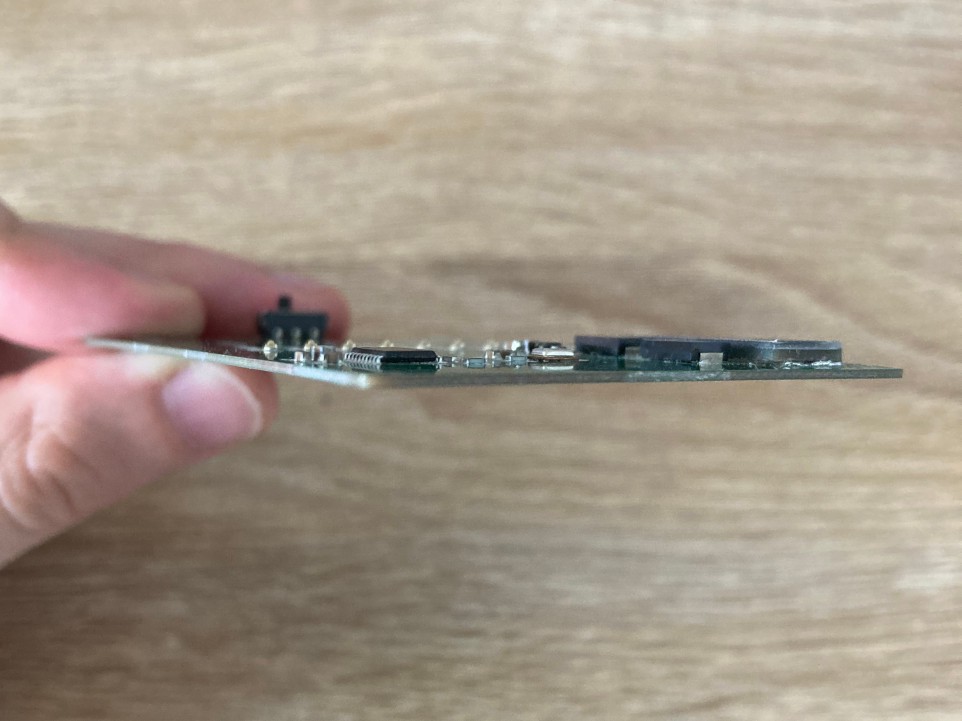
With the 0.8mm thick PCB, the card is overall very thin. It's 3mm thick including the solar cell, and a bit beyond that with the on-off switch. Another change to consider would be swapping the switch for a thinner tactile button.
For testing, I powered the microcontroller with an external power supply; either 1.8V on VCC or 2.5V at the solar cell. My programmer (an Olimex ARM-USB-OCD-H) connected to the MCU just fine, and I was able to flash firmware and get started on software bringup. I'll cover that and have notes on testing in the next post.
Discussions
Become a Hackaday.io Member
Create an account to leave a comment. Already have an account? Log In.