This is the first block of modular sensing system that I'm building.
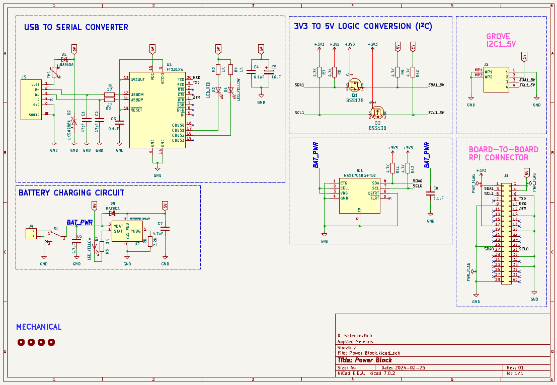
The first thing to do is after finishing the schematics and layout is to order the PCBs. I worked with PCBWay for several years and I am always satisfied with their service and high-quality PCBs.
After a few days a beautiful blue PCBs with ENIG surface finish and stencil for solder paste application arrived.
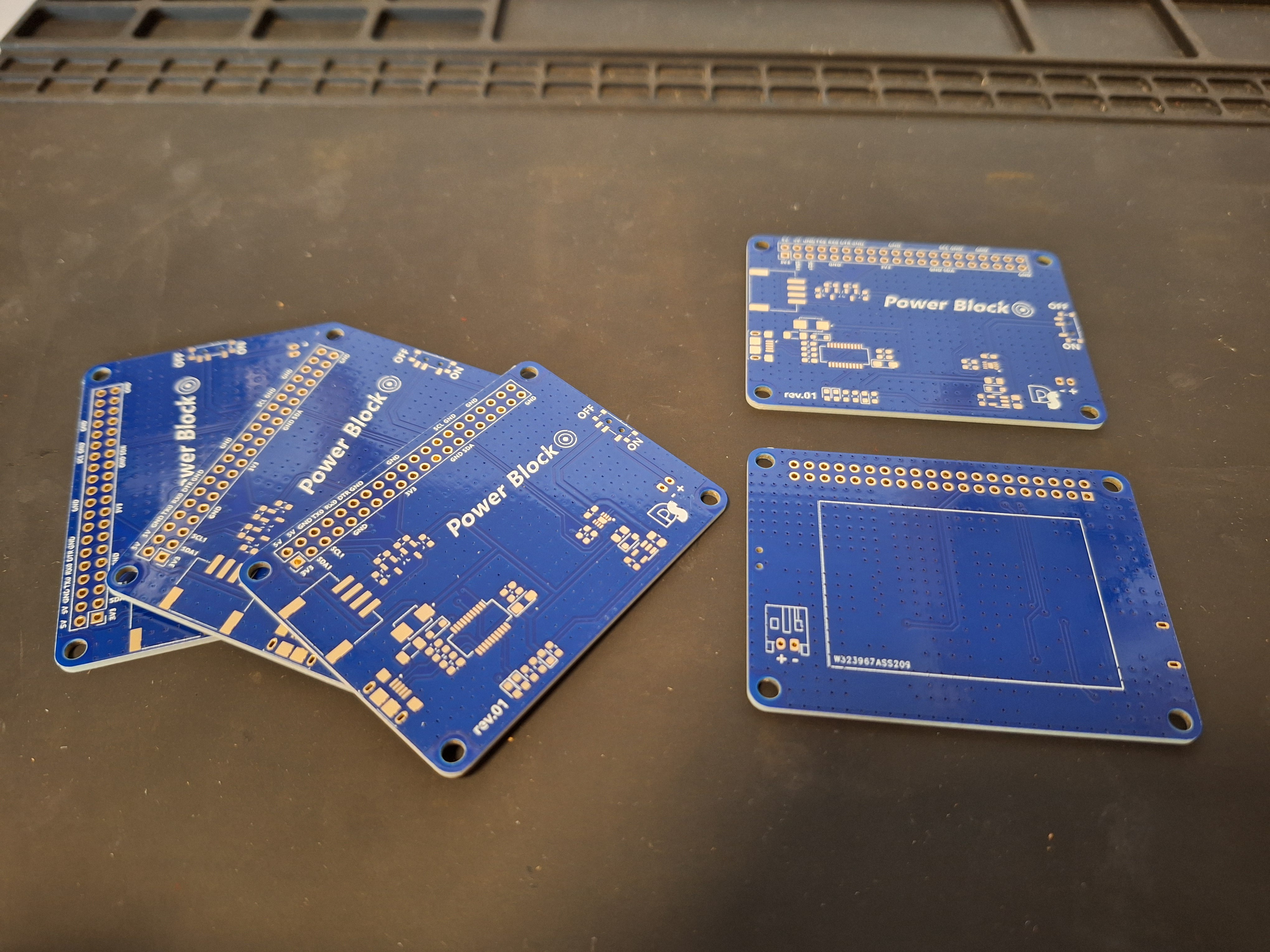
I like to make the PCB assembly by myself at my home lab. I find it most efficient method to test my designs.
Step 1: Solder Paste Application
Making sure that PCB is secured in place and is not moving. I like to pad the PCB with similar height PCBs to make sure that the stencil will be on a flat surface. I use masking tape to secure the PCB in place.
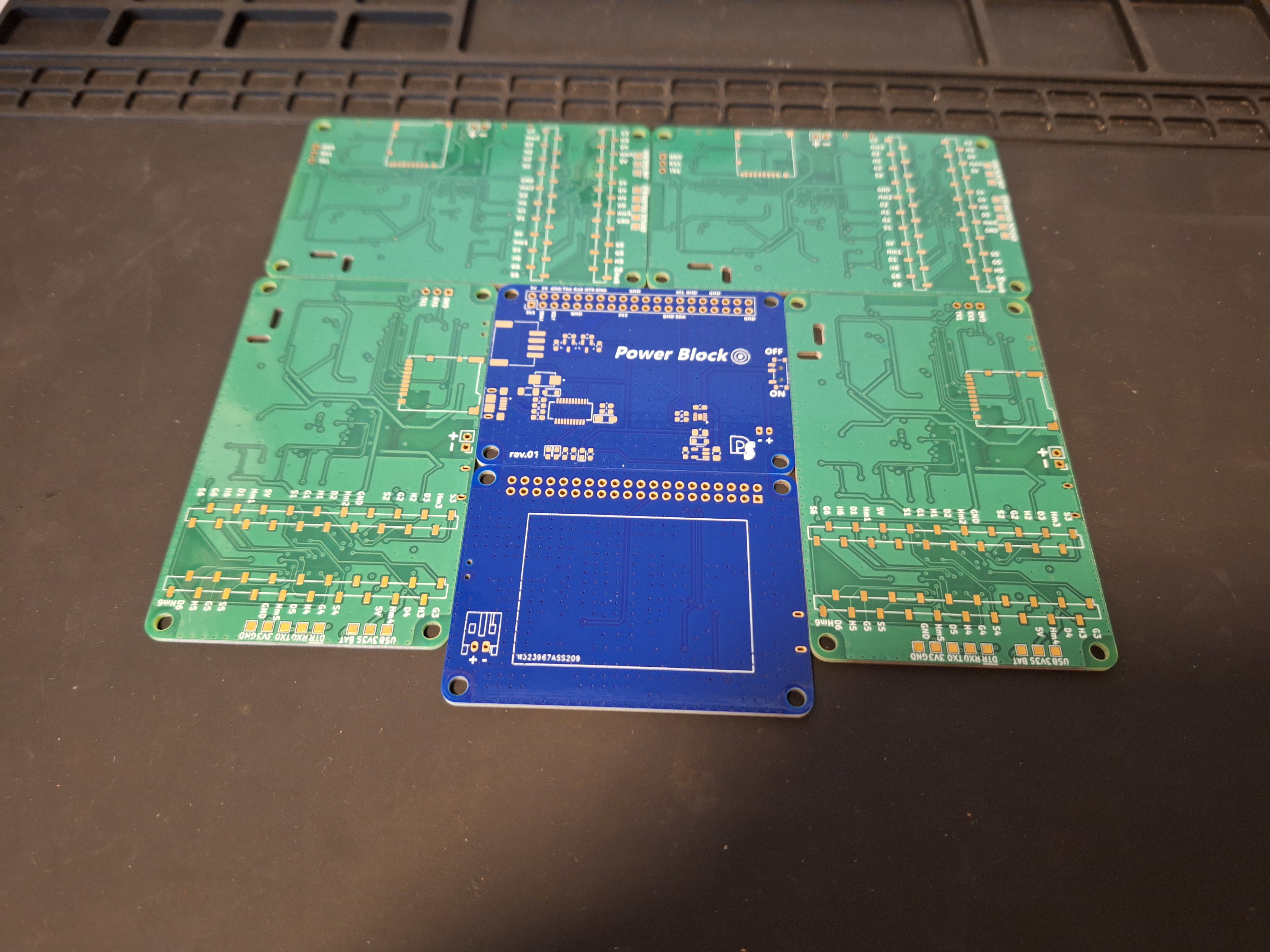
Using the same masking tape to secure the stencil in place. Now the assembly for solder paste application is ready.
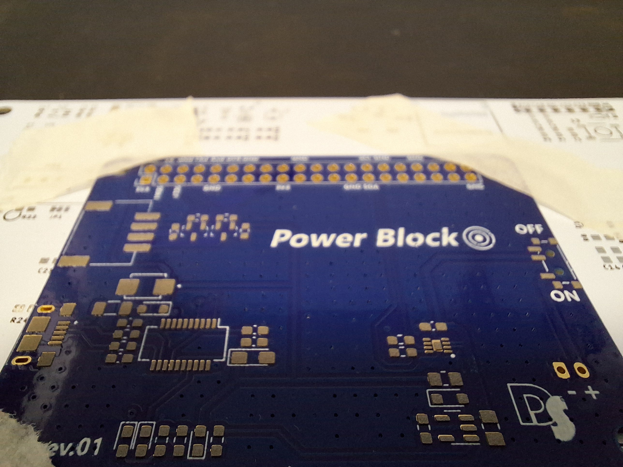
After solder paste application, the stencil is removed and the solder paste on the PCB pad is looking good (great success).
Step 2: Component Placement
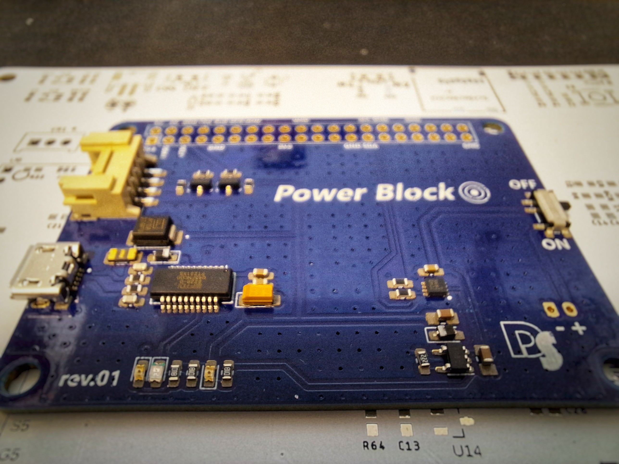
It is essential to secure the PCB on some surface bigger than the PCB itself. In such way you will be able to rotate the PCB during the component placement without touching it.
Step 3: Reflow Time
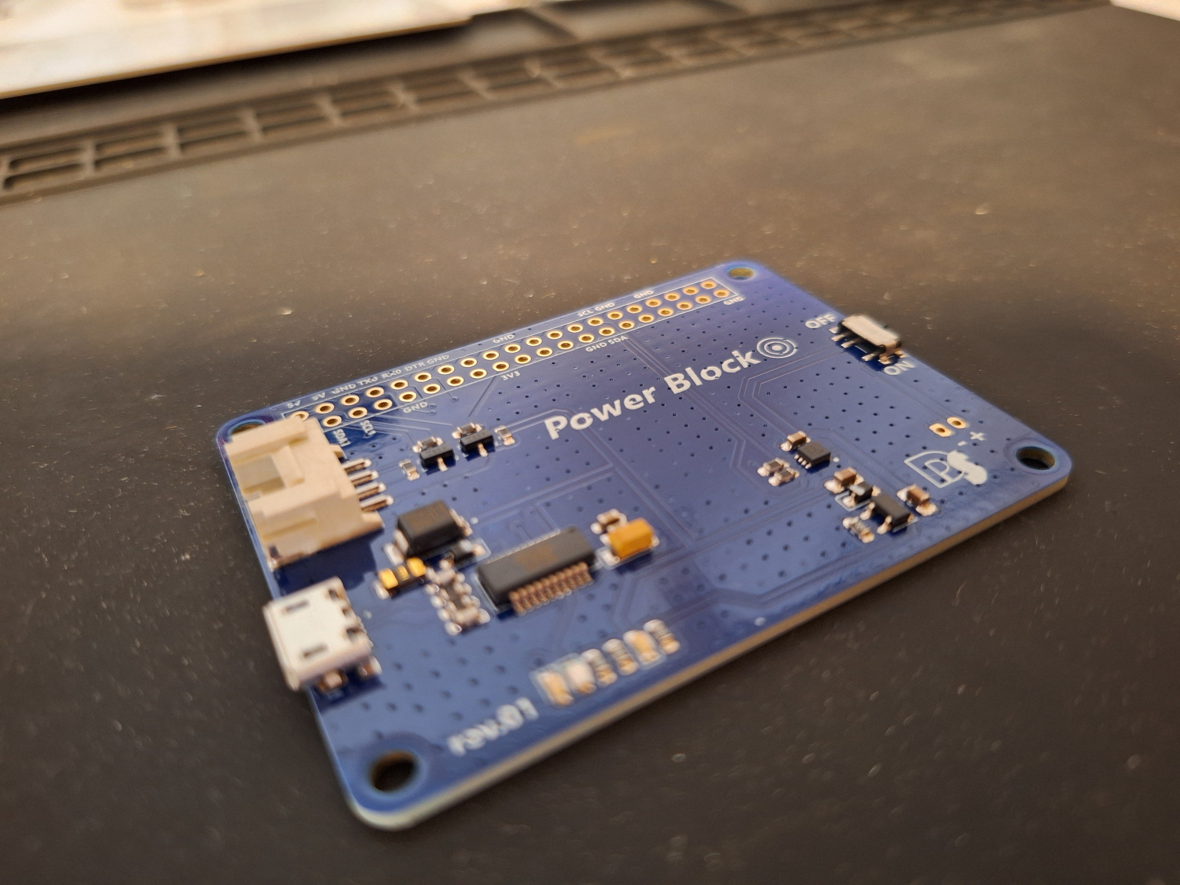
I use my homemade reflow oven but is also possible to use a hot plate to reflow the PCB. It is critical to inspect the PCB after the reflow, especially the fine pitch ICs. Rework is sometimes required to remove short circuits.
Step 4: Manual Soldering of through hole components
PCB holders are great tools for manual soldering. I like these fellows.
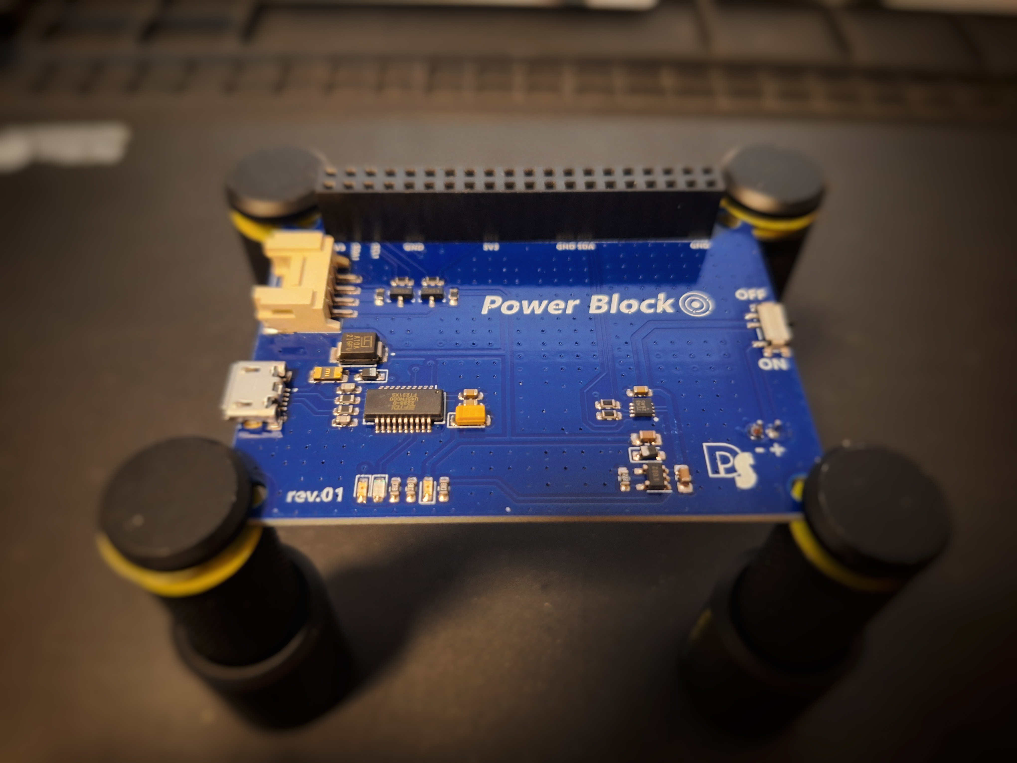
Well done. The assembly is finished.
Discussions
Become a Hackaday.io Member
Create an account to leave a comment. Already have an account? Log In.