 Mitsuru Yamada
1. Overview
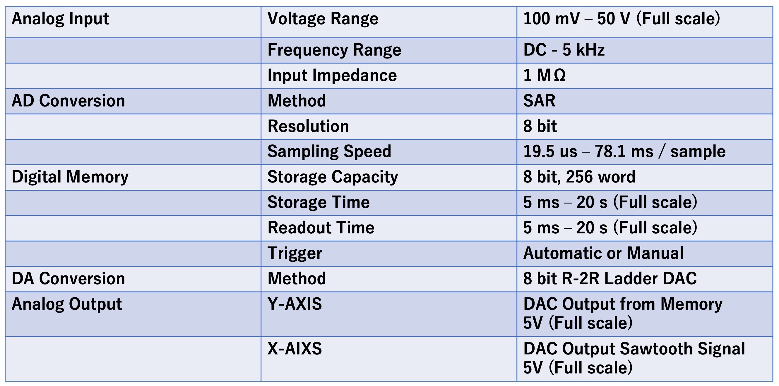
Figure 1 shows the appearance of this Digital Sampler and Table 1 shows the specifications. This device is the origin of my Homemade Successive Approximation Register ADC project (2021). The aluminum plates on the top and sides of the enclosure have been removed. The external dimensions without knobs and other protrusions are 150 mm x 200 mm x 265 mm. The analog oscilloscope on the right side shows the sampled waveforms. I recently posted a video of the internal configuration of this device on YouTube. And it was featured on Hackaday's top page blog. This article presents a video of the actual operation of this device and explains its internal circuitry.
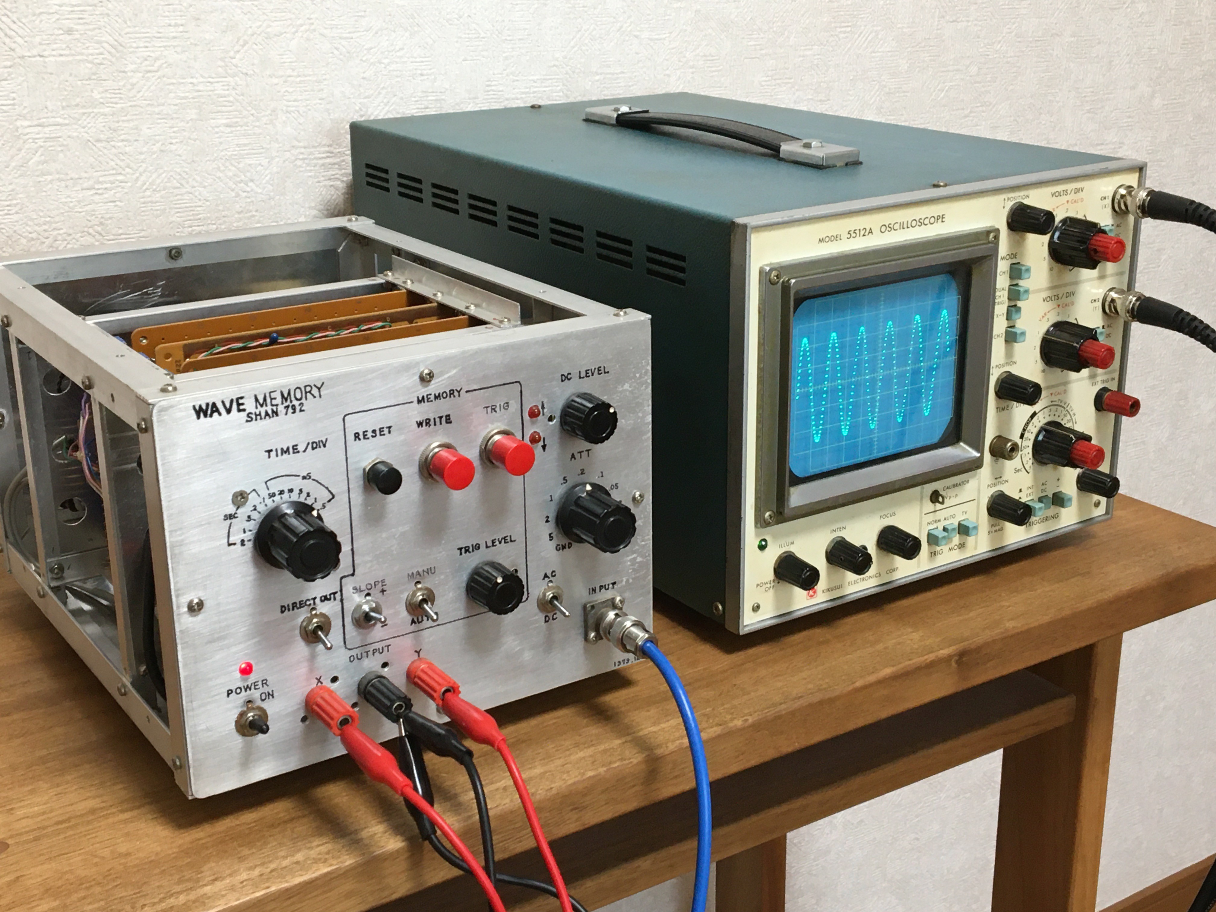
Fig. 1 Appearance of this Digital Sampler.
Table 1 Specifications of this Digital Sampler.
2. Operation example
Video 1 below shows a basic operation example of this Digital Sampler. The input analog signal is the signal from the function generator on the left side of the screen. The analog signal is sampled and stored by the Digital Sampler and displayed on the analog oscilloscope on the right side of the screen. The 500 Hz input signal is sampled with a sampling period of 39 us. And we can see that the input attenuator and DC level adjustment changes the over-range LED display. And it can be seen that the signal level at the acquisition start point on the left end of the oscilloscope waveform changes as the trigger level is adjusted. Then, when the Write button is pressed, the stored signal waveform is displayed in steady state.
Next, I will show how the display changes when the input signal frequency is increased from 500 Hz to 2 kHz and when the sampling rate of the Digital Sampler is slowed down. Furthermore, the frequency of the input signal move to set 24.5 kHz, which is almost the same as the sampling period. You can see that the alias phenomenon caused by the Nyquist theorem results in the display of a sine waveform that does not exist. The last part of the video shows sampling with square wave and ramp waveforms.
Video 1 Introduction of actual operation examples of the Digital Sampler.
(This video does not have audio commentary, so please turn on subtitles.)
3. Circuit configuration
Figure 2 shows a block diagram of the entire circuit.
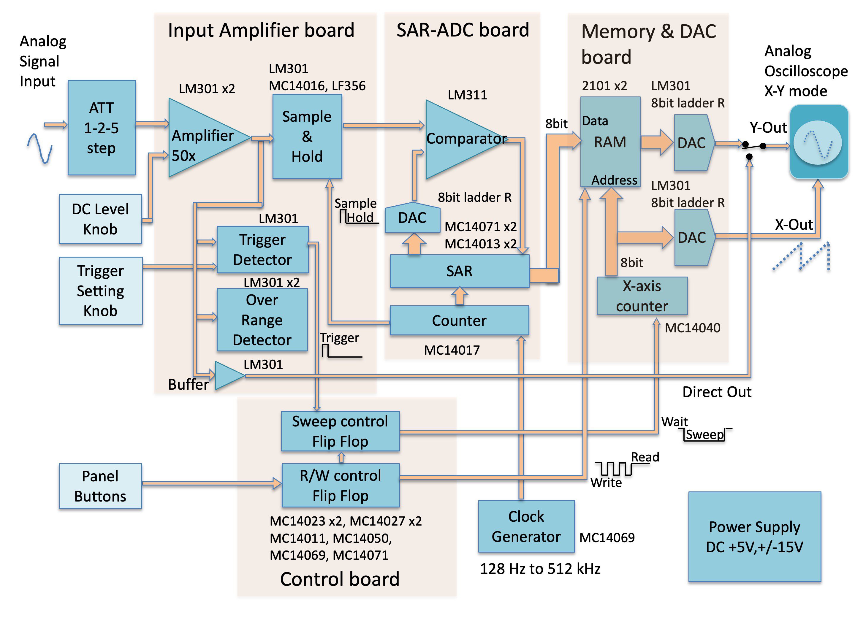
Fig. 2 Block diagram of the Digital Sampler.
First, the analog signal is adjusted to the appropriate amplitude with the 1-2-5 step attenuator on the panel knob. Then, the input amplifier board amplifies the signal with a gain of 50 times and performs sample & hold. The sample & hold is necessary because if the input voltage changes during AD conversion, the conversion result will not be correct. DC level adjustment of the signal, trigger detection and overrange detection are also performed on this board.
Next, AD conversion to 8-bit values is performed on the SAR-ADC board, using a SAR (Successive Approximation Register) ADC as the AD conversion method. Since inexpensive monolithic IC AD converters were not common at that time, the SAR-ADC was made by myself using discrete circuits. The sampling period could be switched in 12 steps of 1-2-5. The fastest sampling period was 19.5us, and the Nyquist frequency was 26kHz. Therefore, waveforms are clearly visible up to a few kHz. No anti-aliasing filter is provided.
After the 8-bit value of the AD conversion result is once stored in the memory IC, it is converted to an analog signal again by a DA converter and displayed on the oscilloscope. Here, the sampled signal is output on the Y-axis of the analog oscilloscope in XY mode, and the sawtooth waveform is output on the X-axis.
If the trigger mode is set to automatic and the trigger level is adjusted to an appropriate value, the input analog signal is stored in memory from the moment it reaches that value. 256 samples later, the bright spot returns to the left edge and waits for the next trigger; pressing the Write button disables trigger detection from the next time and stores the stored signal continues to be displayed.
Figure 3 shows the operation panel and the internal boards configuration. And Video 2 shows the internal structure from various angles. The input amplifier board is fixed to the internal partition sheet metal behind the operation panel. The card cage behind it contains, in order from the front, the SAR-ADC board, the memory & DAC board, and the Control board. The power supply section is fixed to the rear partition sheet metal behind it. The chassis is made of aluminum L-angles and aluminum plates. The card cage part was also made by myself with L-angles.

Fig. 3 Operation panel and the internal boards configuration.
Video 2 The Digital Sampler internal structure from various angles.
4. Circuit configuration
4-1. Input Amplifier board
The circuit diagram of the input amplifier board is shown in Fig. 4. The operational amplifier LM301, which was common at the time, is used for amplification. For trigger detection and overrange detection, LM301 is used in an open-loop connection instead of a dedicated comparator IC. The sample & hold function is used to prevent incorrect AD conversion values if the signal voltage changes during AD conversion. The sample & hold is composed of an analog switch MC14016, a capacitor for hold, and a FET input operational amplifier LF356. The operating waveform of the sample & hold is shown in Fig. 5-1 below. The appearance of the board is shown in Fig. 5. The printed circuit board is a double-sided board, and the wiring pattern fabrication process was done by me using a ferric chloride solution for etching.
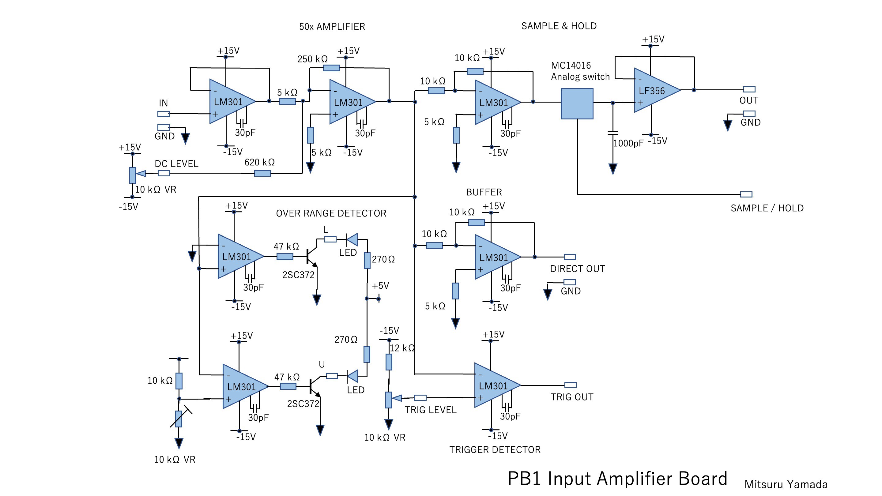
Fig. 4 Circuit diagram of the Input Amplifier board.
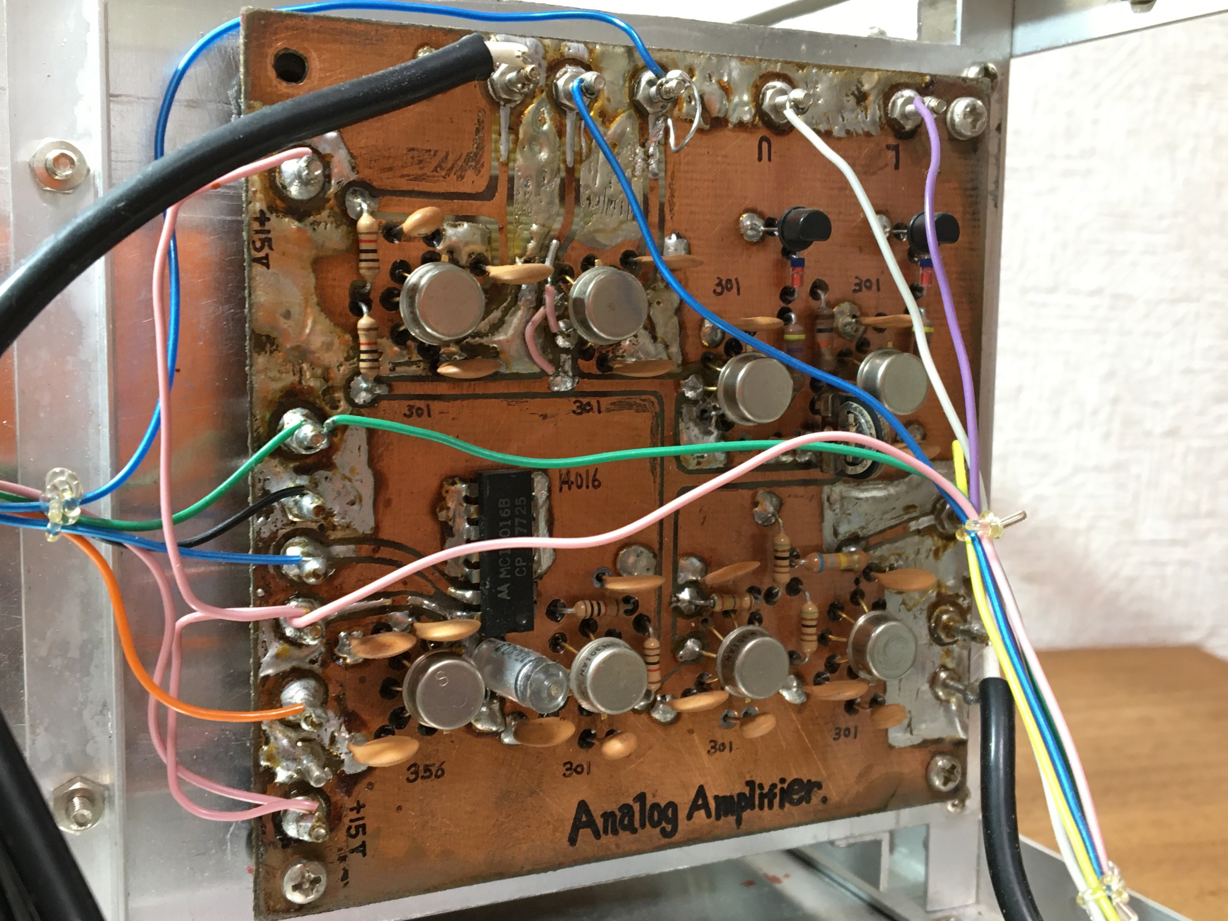
Fig. 5 Input Amplifier board.
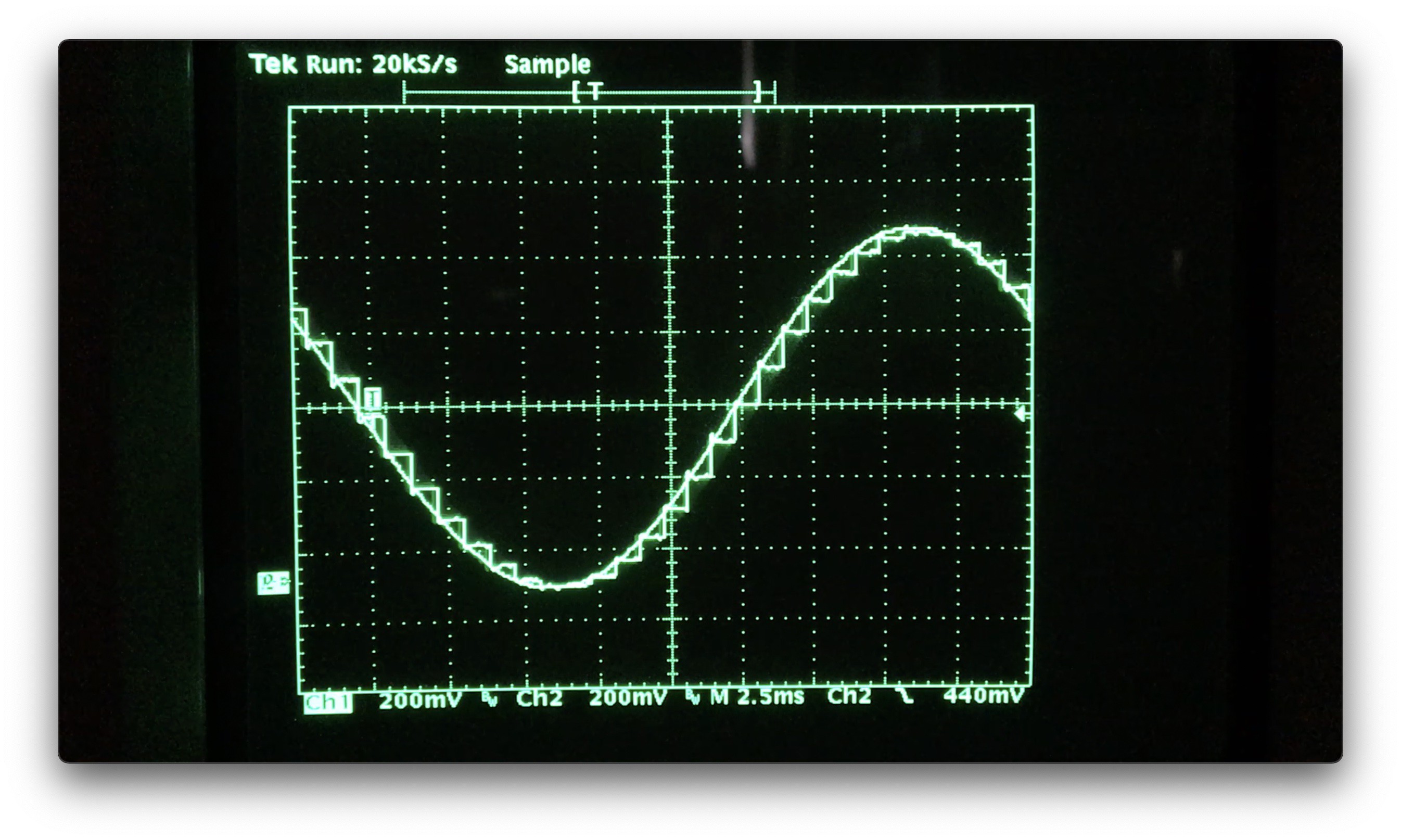
Fig. 5-1 Sample & Hold waveform.
4-2. SAR-ADC board
The circuit of the SAR-ADC board is shown in Fig. 6, and the component side of the board is shown in Fig. 7. The wiring side is shown in the photo gallery of this project. The circuit board was a universal PCB, and the wiring was done by soldering. The MC14000 series CMOS standard logic ICs were used as the digital element. Comparator LM311 compares the analog signal voltage input to ANALOG IN with the output voltage of the DAC composed of an R-2R ladder.
The counter for sequencing from the upper bits of SAR is the decimal Johnson counter MC14017. Each time a clock pulse is input, the Johnson counter outputs a H-level signal of the clock pulse width from Q0 to Q9 in sequence to the SAR. The result of the OR operation of that signal logic and the signal logic held by the D flip-flop becomes the input of the DAC. The comparator comparison result is held in the D flip-flop MC14013 in order from the upper bit.
The generation of the 8-bit AD conversion value is completed with nine pulses from the Johnson counter outputs Q0 to Q8. Then, the next pulse of Q9 holds the sample hold, initializes the DFF of the SAR, and resets the sweep generator. After this, the conversion process is repeated again from the Q0 output.
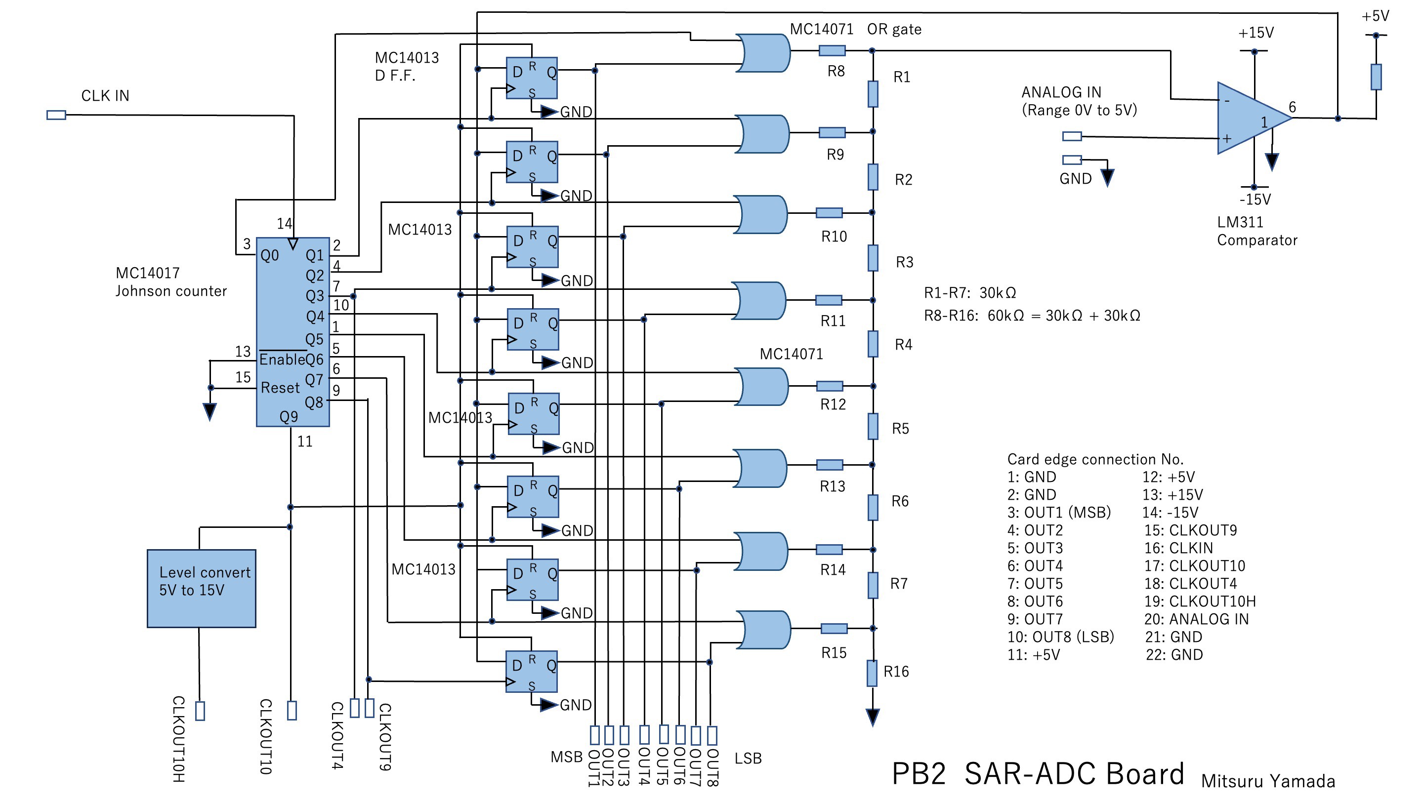
Fig. 6 Circuit diagram of the SAR-ADC board.
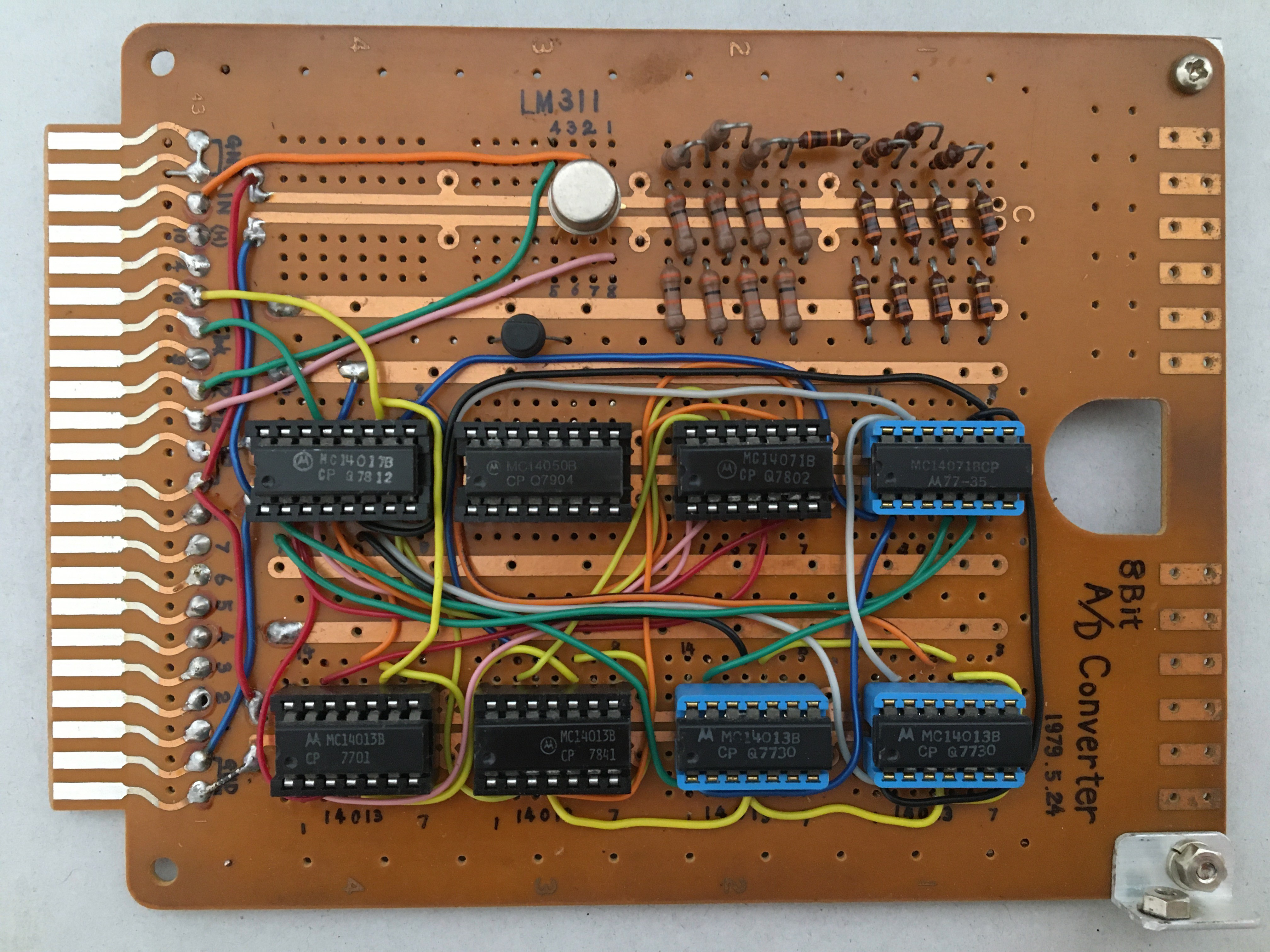
Fig. 7 The SAR-ADC board.
The conversion process of SAR-ADC, where the ladder resistor DAC output converges to the analog input voltage step-by-step with a 78.1 us clock cycle, is shown in Video 3. In this video, the input signal is a ramp waveform that goes up and down over 10 seconds. This signal is held during the AD conversion convergence operation by the sample & hold.
Video 3 Conversion process of the SAR-ADC.
4-3. Memory & DAC board
Figure 8 shows the circuit of the Memory & DAC board, and Fig. 9 shows the component side of the board. The wiring side is shown in the photo gallery of this project. 8-bit data from the SAR-ADC is stored sequentially in a 256-byte memory. This memory consists of two 4-bit x 256 1kbit SRAM 2101s. At the time, in the late 1970s, semiconductor SRAMs were revolutionary even with this kind of capacity. In this SRAM, the input data bus and output data bus are independent, so the output data bus outputs the written value as it is. This output is reconverted to an analog signal by a DAC composed of an R-2R ladder and an operational amplifier, and is used as the Y-axis output to an analog oscilloscope.
A binary counter MC14040 is used as the sweep generator. This counter counts up every sample. The CLKOUT4 (Johnson counter Q3) output of the SAR-ADC board is used for the clock. The 8-bit value that this counter counts up is converted into an analog sawtooth signal by the DAC, and the signal is for the X-axis output. The count-up value of this sweep generator is also used as the memory address input. Fig. 9-1 shows an example of Y-axis output and X-axis output waveforms. And Fig. 9-2 shows that signal displayed in X-Y mode.
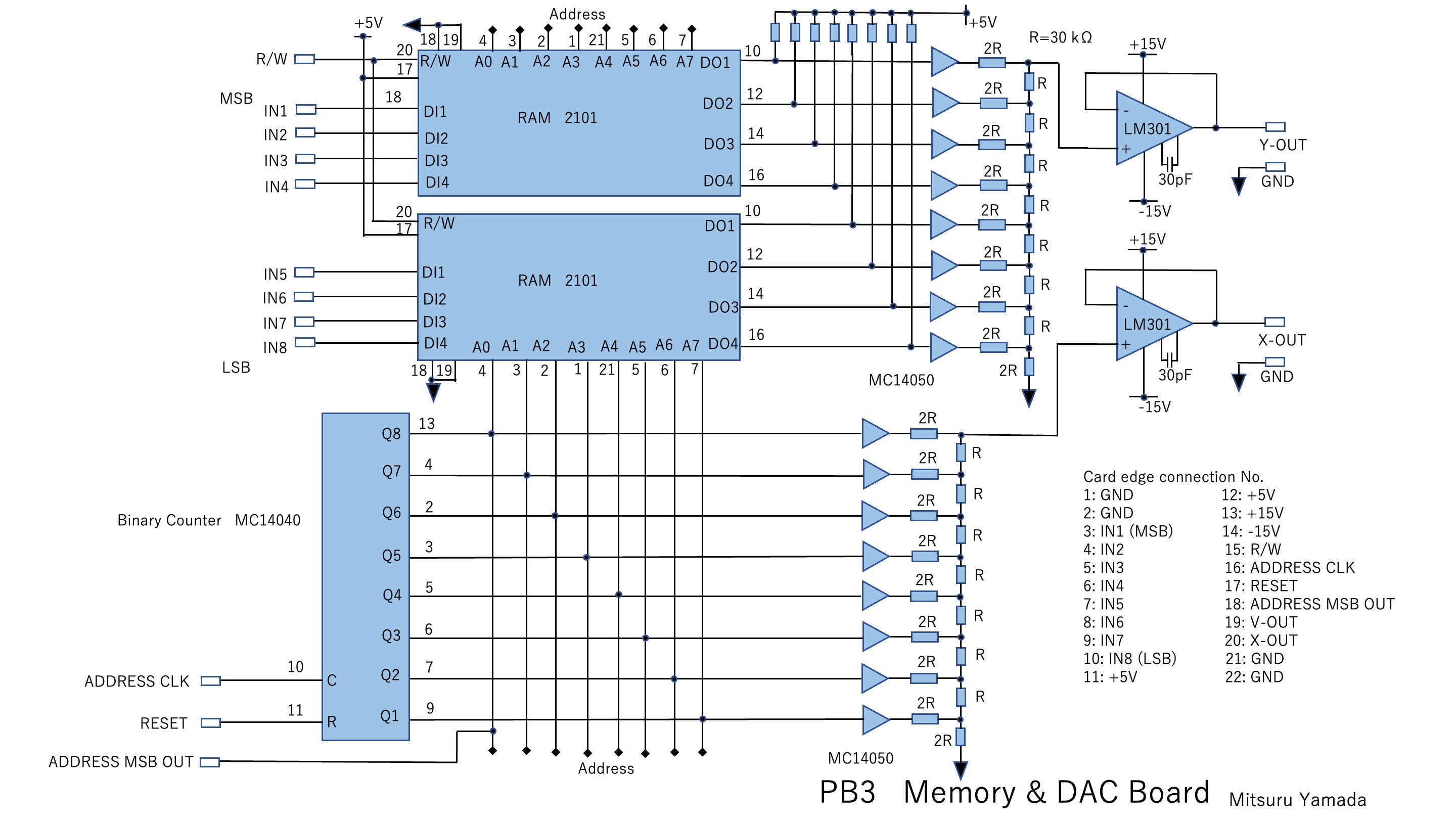
Fig. 8 Circuit diagram of the Memory & DAC board.
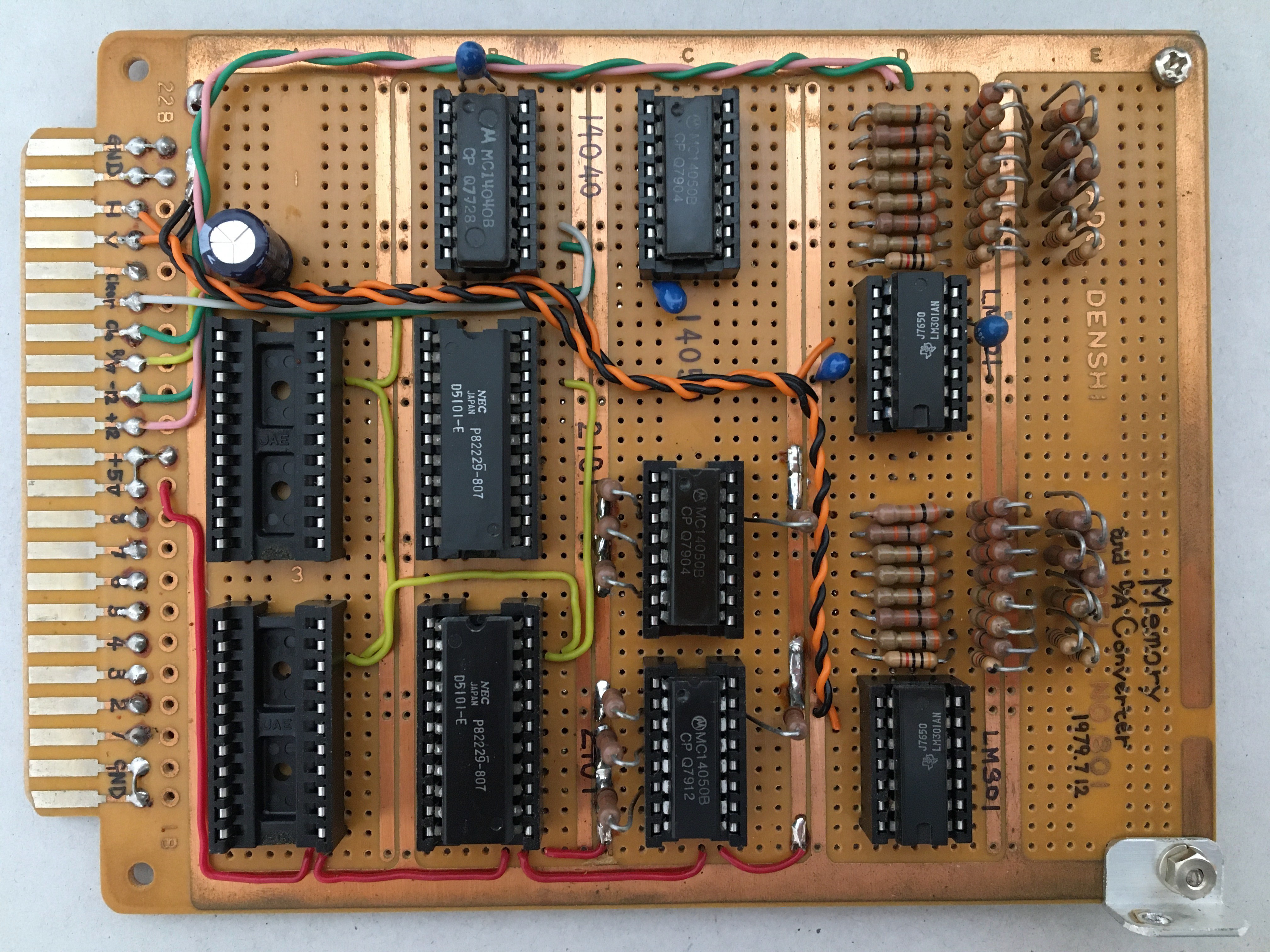
Fig. 9 Memory & DAC board.

Fig. 9-1 Waveforms of Y-axis output and X-axis output.
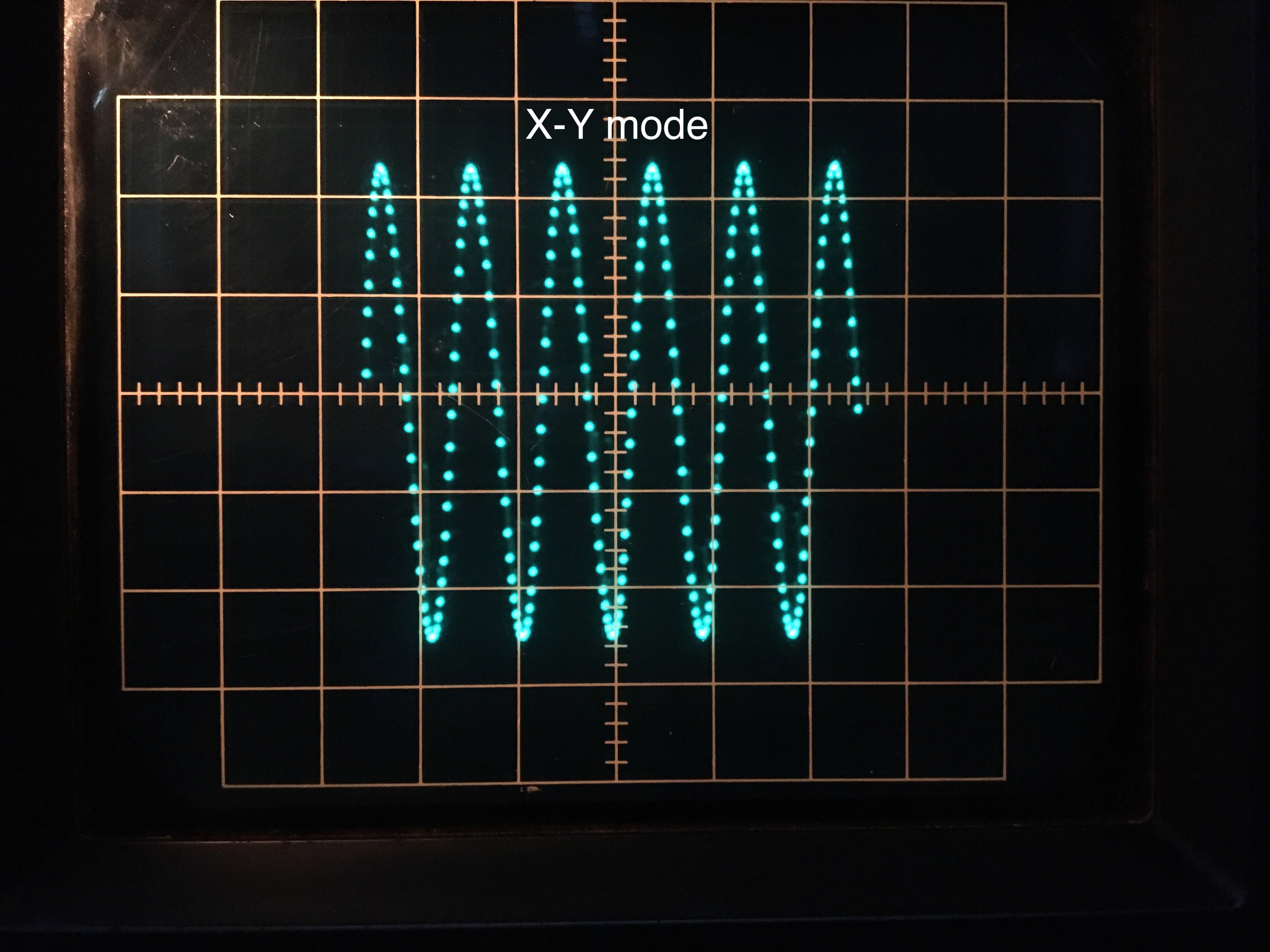
Fig. 9-2 The signal in Fig. 9-1 displayed in X-Y mode.
4-4. Control board
Figure 10 shows the Control board circuit and Fig. 11 shows the component side of the board. The wiring side is shown in the photo gallery of this project. For the trigger signal from the trigger detector on the input amplifier board, the logic is processed to be non-inverted or inverted depending on the positive or negative slope setting. When the trigger mode switch is set to AUTO, this signal sets the sweep control FF to the set state. If the trigger mode switch is set to MANUAL, the pulse from the TRIG button sets the sweep control FF. This releases the sweep generator reset and the X-axis sweep is performed. The sweep control FF is cleared by the sweep generator's address MSB signal, and the sweep is terminated, and the sweep enters the wait state.
When the WRITE button is pressed, the R/W control FF is set, and memory write in the next sweep is inhibited. This means that the waveform data stored in memory will continue to be displayed in subsequent sweeps without being overwritten.
The removal of signal bounce from the panel pushbutton switch is simply configured with a positive feedback circuit that connects the input and output of the non-inverting buffer MC14050.
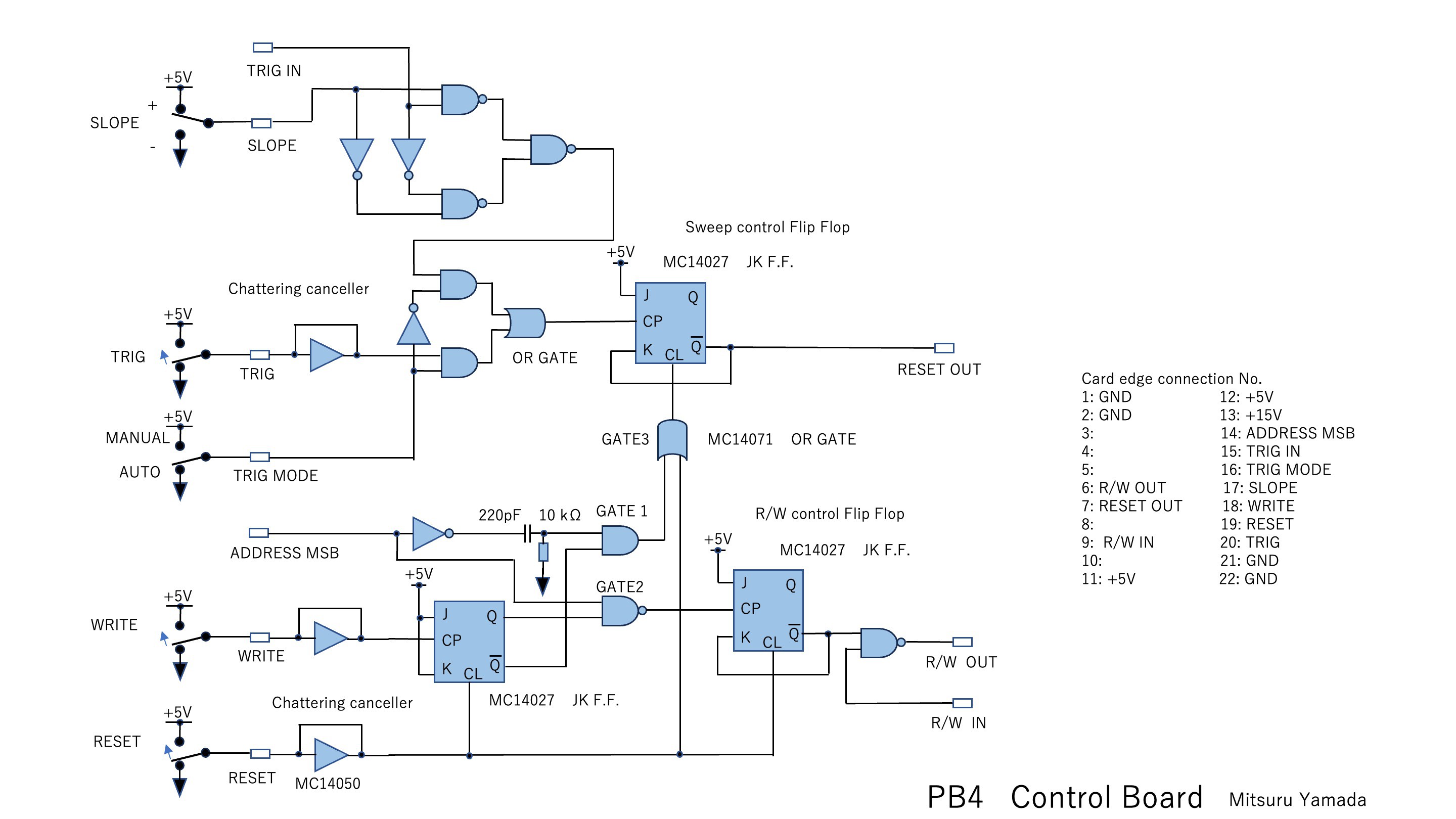
Fig. 10 Circuit diagram of the Control board.
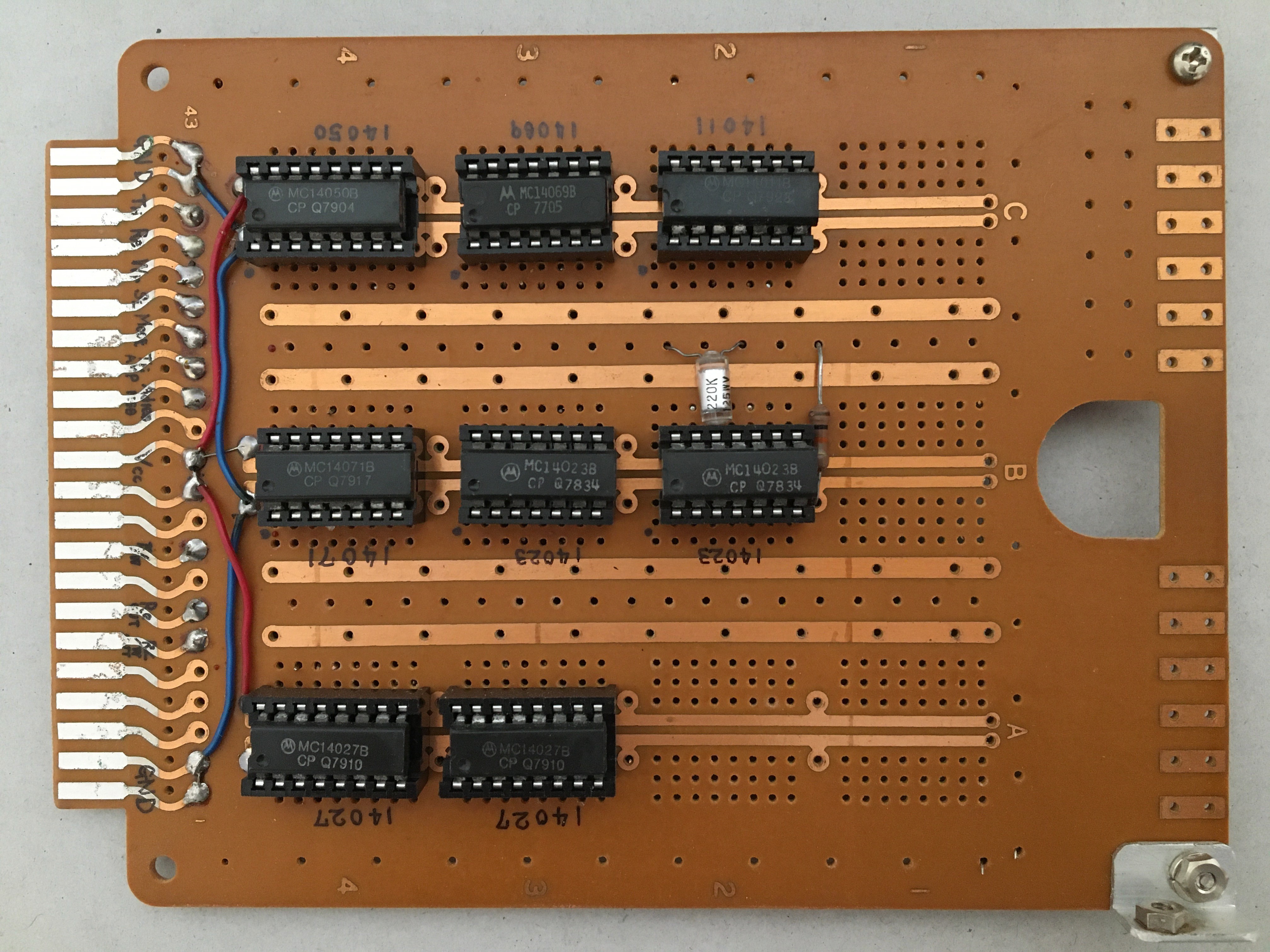
Fig. 11 Control board.
4-5. Clock generator
The circuit of the clock generator is shown in Fig. 12, where the period of the basic clock itself is switched in 12 steps in order to be able to switch the sweep time in 12 steps of 1-2-5 steps. Although the oscillation circuit is not very stable, it is simply composed of a CR oscillation circuit. Therefore, when the sweep time is made slower, the AD conversion clock becomes slower and the AD conversion time becomes longer. Although the hold time of the sample hold also becomes longer, this method was used to simplify the entire device. Originally, it would be preferable to keep the AD conversion time constant even if the sweep time is changed.
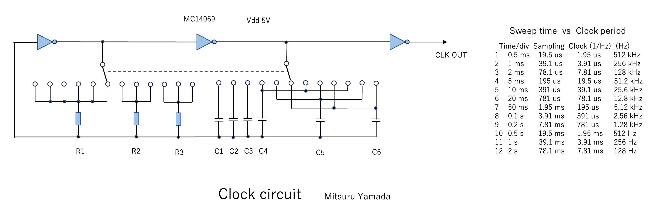
Fig. 12 Circuit diagram of the clock generator.
4-6. Operation panel
Figure 13 shows the operation panel wiring side. This photo shows the front panel removed from the enclosure frame.
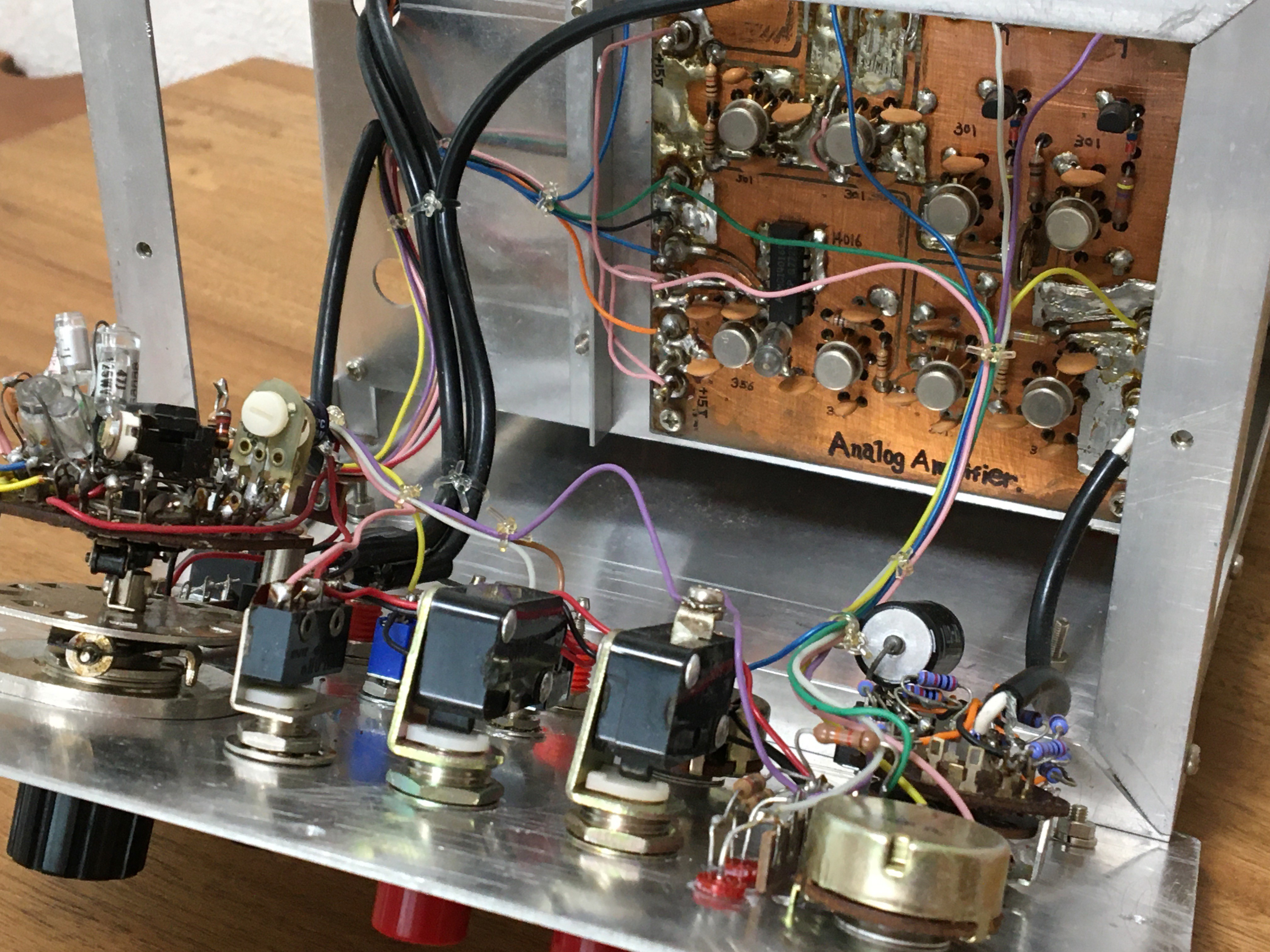
Fig. 13 Wiring side of the operation panel.
4-7. Power supply
Figure 14 shows the power supply section. The power supply section used a transformer and a 3-terminal regulator IC to generate the circuit power supply voltages of +5 V DC, +15 VDC, and -15 V DC from 100 V AC.
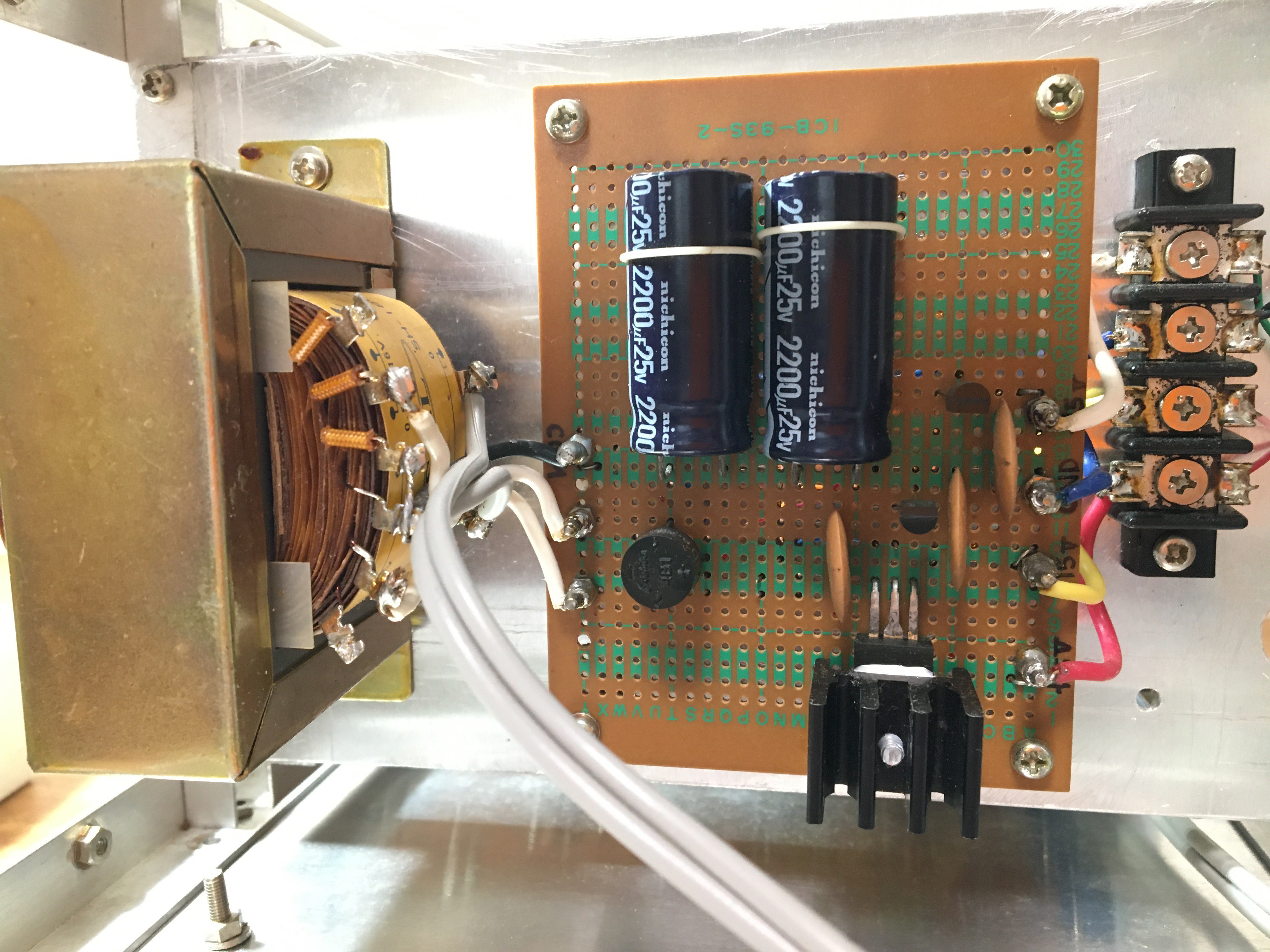
Fig. 14 The power supply section.
5. Failure repair
This device was completed in December 1979, but was stored at my parents' house from 1985 to March 2024. After examining the signal waveforms of each part of the board, I was able to pinpoint the defective part to a single pin on the IC. It was found that whisker growth from the tin-plated surface of the pin was causing a short circuit with the other pin. The resistance between that pin and the adjacent pin was 15 ohms due to the short circuit caused by the whisker, even though the correct resistance value is usually on the order of mega ohms.
The IC was replaced with a new one and the device was confirmed to be working properly. A photograph of the whisker is shown in Figure 15, which shows the third and fourth DIP package IC pins from the right connected by the whisker. Roughly speaking, if the whisker growth rate was 0.9 mm over 45 years, one atom of thickness would have been pushed out every 10 minutes or so. It was an important experience for me to discover the IC failure caused by whisker growth after 45 years in a device I built myself.
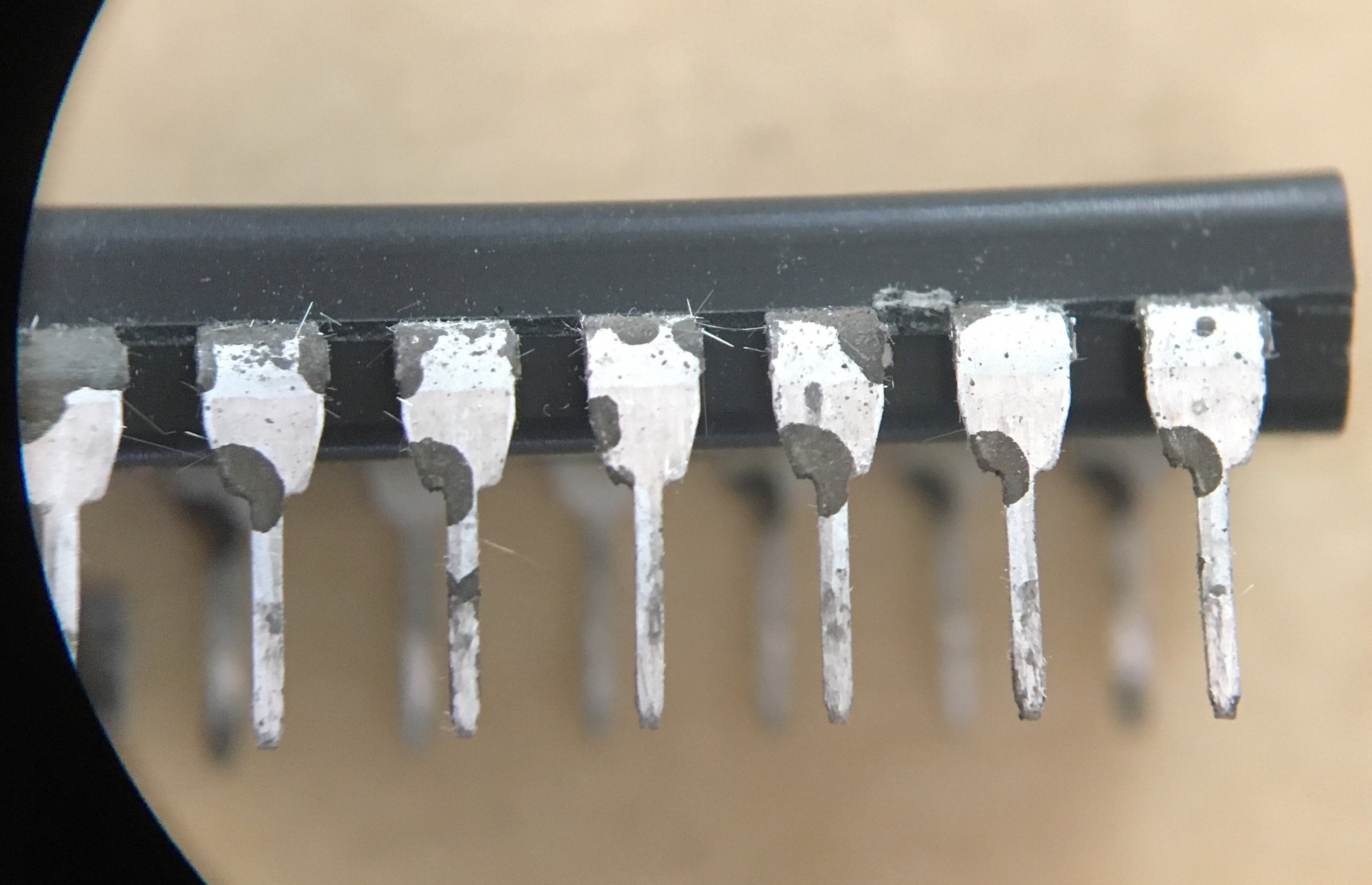
Fig. 15 Short circuit due to whisker between IC pins after 45 years.
6. Results
In 1979, each circuit was built by experimenting a little at a time, so the entire project took 8 months to complete. The maximum sampling rate was 19.5us, so it was possible to save single-shot phenomena with frequencies up to several kHz, such as voice, and observe them with an analog oscilloscope. An example of an observation of a single-shot phenomenon captured by a microphone when a desk was tapped is shown in Video 4. However, I felt that this sampling rate needed to be increased by a factor of 1000 more when trying to observe a single-shot control signal with a clock signal of about several MHz of a microcomputer, which was beginning to boom at the time. It would be nearly 20 years later, around 2000 AD, that this would be realized with a digital oscilloscope at a price that could be purchased by an individual.
Video 4 A shingle-shot capture example. (This video does not have audio commentary, so please turn on subtitles.)
This device was very convenient to experiment with various frequencies of input analog signals and sampling periods of the device, and to experience sampling theorems and aliasing phenomena in real time. I still clearly remember my surprise when I was able to observe these phenomena in real time. In the end, the significance of the device as an experimental device of principle was more important to me than its practicality as a digital sampler. After this, I went on to a life of developing signal processing equipment.
References
[1] Transistor Gijutsu, CQ Publishing Co., Ltd, Sep. 1978 issue etc.
(Posted on Jun. 28, 2024)
(Latest revision on Jul. 09, 2024)