Close
0%
0%

Boost Converter Development Board

A breadboard-compatible DIY dev board built on the TPS61022 chip.

Similar projects worth following
216 views
I wanted to play around with boost converters for driving an ESP32 with a single 1.5v battery and had my eye on the TPS61022 chip from Texas Instruments. When it arrived, I immediately realized this wasn't at all a hand soldering job.

As I'm also wanting to better my PCB design skills, I took a crack at making a more versatile development board able to produce a range of step-up voltages. While the AliExpress boost converter development boards are fairly cheap, they are also bulky and not very breadboard-friendly.

This would be a pretty good project if you're wanting some practice with SMD soldering fine pitch components, or like myself, want to add another interesting development board to your arsenal.

NOTE: I'm currently working on curating the files/tags on Github in order to match the version numbers that are posted here.

Check the files in this project for the gerber zip which can be uploaded to JLCPCB (or any other pcb fabricator). No special pcb instructions are needed for this board.

v0.2 is currently in progress (see first picture in the gallery). As of 6/30 I actually have the PCB + parts and just need to find the time to assemble it. Will post a worklog once that's done.

boost-conv-v0.1-gerbers.zip

v0.1 pcb production exports

Zip Archive - 33.68 kB - 06/30/2024 at 18:08

Download

  • 1 × Texas Instruments TPS61022RWUR Switching Chip
  • 1 × Bourns SRP6030VA-1R0M Inductor
  • 1 × 1x 10uF Ceramic Capacitor (C1)
  • 1 × 3x 22uF Ceramic Capacitor (C2-C4)
  • 1 × 732k 0805 SMD Resistor (R1)

View all 6 components

  • v0.1 - Getting my feet wet

    Nathaniel06/30/2024 at 17:58 0 comments

    The first iteration of this design honestly isn't even an iteration.

    I know the final product I'm looking for is nothing like what v0.1 turned out to be, but I needed to know that I could:

    1. Solder the chip to the board
    2. Design a capable board
    3. Select the correct components for proper functionality

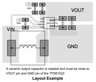
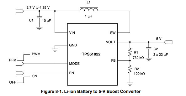
    I'll give full credit to the TPS61022 datasheet, which directly gives (thank you TI) a recommended pcb layout along with an example circuit which input a ~3V signal and output 5V, conveniently close to my original use case:

    They really made my life easy. I opened up Kicad, copied the schematic over, and laid my pcb exactly how the datasheet showed. They do stress a few things such as the distance of the capacitors to the TPS61022, but other than that, it seems pretty straightforward. For the inductor choice, there wasn't too much thought put into this other than this snippet from the datasheet: The TPS61022 is designed to work with inductor values between 0.33 µH and 2.9 µH.

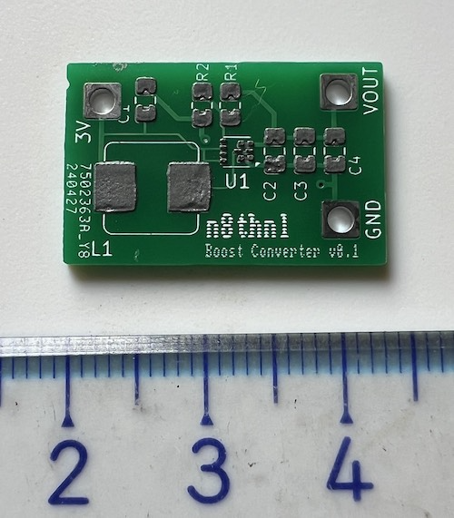
    This was actually the first pcb I'd designed from scratch, hence the absence of a ground plane and a single trace on the bottom layer. The design rules checked out, though, so I exported the production files, uploaded them to JLCPCB and a few weeks later got the bare pcbs. 

    I ordered a stencil for this, because, well you need one. For stencil alignment, I 3d printed a small jig to hold both the board and stencil in place while I pushed the paste through. 

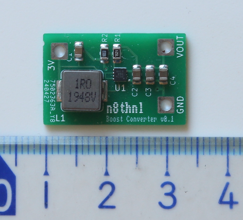
    After that, the components were placed and off to the hot plate. I turned it up to 200 C and once I got that nice flow, I shut it off, let it cool, and could finally test it!

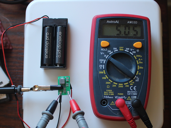
    Now, I don't have an oscilloscope, so I can't zoom into the output voltage waveform, but a stable reading on the multimeter is good enough for me to start work on v0.2.

    Also note that I didn't actually pass through any load, so again, I'm not aware of the limitations or even the performance of this setup once it's actually in use.

View project log

Enjoy this project?

Share

Discussions

Similar Projects

Does this project spark your interest?

Become a member to follow this project and never miss any updates