 Gangwa Labs
This Dev Log is pulled straight from my notes
Goals
- understand how NPN and MOSFET fit together to create a cheap control signal for the higher power PCB hotplate
- Understand how the example Hotplate schematic works
Simplified Schematic
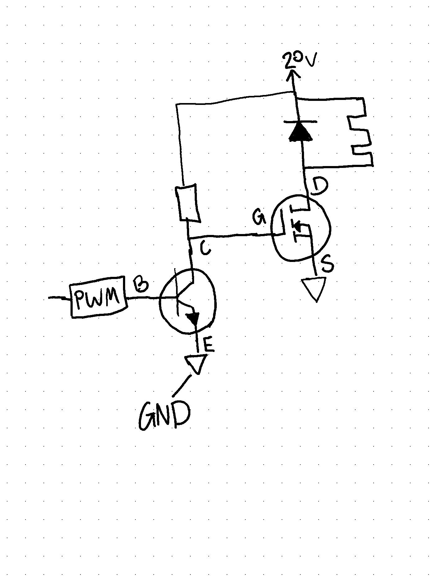
- NPN Transistor is acting as an inverting Switch ie. LOW from the PWM is 100% power
- When the NPN Transistor is turned on the Gate of the MOSFET is brought to ground via the collector-emitter path and this turns off the MOSFET
- When the transistor is off the voltage at the gate is higher than the Source(GND) and the current is free to flow through the resistive heater and from Source to Drain completing the circuit
Sourcing Components
MOSFET
- 20V VGS with more than 3A of Drain continuous Current
BJT
- Collector to emitter voltage of 20V
- Collector Current able to withstand more than 3A for safety rating
- Base voltage at 3.3v micro-controller level and able to be controlled with 20mA or less of current
Reading BJT Datasheets
- ??????
Discussions
Become a Hackaday.io Member
Create an account to leave a comment. Already have an account? Log In.