Well, me and PADS Professional didn't fall in love with each other, so that couldn't last forever.
It just became certain that I'm going back to university! Great news, but that means I'm looking for a part-time job... which in Austria is rather rare, so I should better take any shots I can at standing out among other candidates!
Fortunately, there's a big job faire right around the corner in Vienna, jobmesse austria on 13-14.09.2025 (the biggest job faire in Austria).
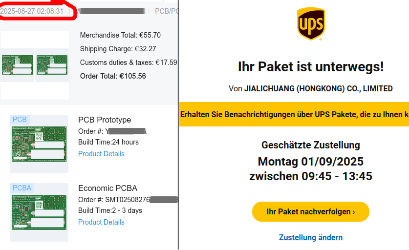
Having expected about 2 weeks lead time on PCB+PCBA, I thought waiting until V1.1 is ready might be a bit risky, so I've ordered 30pcs of V1.0 last Wednesday (27.08)... They're expected to arrive on Monday(01.09)! 🤯.
See you at Jobmesse Austria! I'll bring few extra cards to give out to anyone who recognizes me! 😆
The V1.1 update is due to come out before Career Start 2025, "Austria’s largest Tech-Career-Week" at FH Technikum Wien in 37 days. The first batch might get sponsored and manufactured in Europe by one of JLC's competitors!
5-6 days (including a weekend) from ordering PCBs to getting them manufactured, assembled and delivered is an AMAZING feat, but remember that the first batch did not go as smoothly (2 weeks delay, 12 emails long chain and an extra $18 fee, after I tried to slightly deviate from a standard process to save few bucks on shipping the pogo-pins). You can read the full story in the previous project log entry.
Here's a detailed timeline of the (second) V1.0 batch:
I've stayed up late and placed the order on 2025-08-27, 02:08:31AM local time in Austria (8:08AM in Hong Kong). The clock started ticking.
JLC's advertised standard (non-express) lead times are 24h for prototype PCB production and 2-3 days for (economic) assembly.
T+01h39m: They've verified and prepared the design files.
T+10h20m: PCBs have entered production and were being drilled.
T+26h13m: Final inspection of the finished PCBs.
T+38h41m: PCBA setup
T+38h43m: Reflow soldering
T+40h04m: (SMT-only) assembly finished
T+41h08m: Packaging of assembled PCBs
T+50h55m: Package ready for pick up by UPS
T+81h17m: UPS picks up the package in Hong Kong
T+121h40m: (expected) delivery attempt in Vienna
T+121h51m: (expected) driver marks the package as undeliverable, claims recipient is unreachable without ringing the doorbell or calling (because it's UPS)
T+129h11m: (expected) delivery to a "Handyshop" instead
T+129h24m: (expected) UPS sends an email informing that the package has been successfully delivered
T+129h51m: (expected) The Handyshop closes for the day, see you Monday-Friday 10:00-18:00 lol
Each board still needs about 15 minutes of work on my side (inspection, hand-soldering an inductor, soldering pogo-pins sideways, forming battery contacts out of silver-plated wire and soldering those, programming and calibration at first start, test, clipping-on 3D printed parts, pipetting UV resin into display segments, quick UV exposure, placing the boards on a windowsill for few hours to fully cure the UV resin, final test) so it's great to have few days of extra time.
Discussions
Become a Hackaday.io Member
Create an account to leave a comment. Already have an account? Log In.