 Jesse Farrell
I was lucky enough to get this eval board (the PCB at least) sponsored by PCBWAY. It gave me a chance to test out some of their capabilities and toy with a small panelized design. I typically use JLC for their component library, but nothing wrong with trying out the competition!
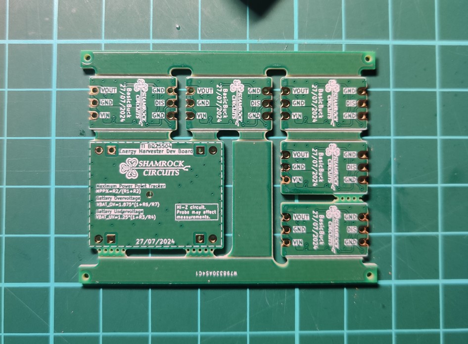
Since there's not too much paneilzation info out there I figure I'd use this log to outline how I did the penalization which includes mouse bites, Vscore, and milling. The panel includes two separate evaluation boards; one for a small buck regulator, and the other a solar harvester IC (this project).
To design the panel, I mostly followed PCBWAY’s panel creation guide. The key takeaways are listed below…
- Route between PCBs: >1.6mm
- V score separation: >2.0mm
- V score min PCB size: 45 x 60mm
- V score PCB thickness: >0.6mm
- Edge Rail width: 5mm (standard)
Manual Penalization in KiCad
In KiCad my workflow for penalization is as follows (yes I know there’s plugins to automate this for simple designs). Note, in my case I’m using two unique PCB’s. One is a solar harvester the other is a little buck converter. Both are essentially development boards.
First step is to design the individual boards as if they were standalone projects. Once you’ve completed all you last checks on those designs start one new KiCad project that will hold the penalization data.
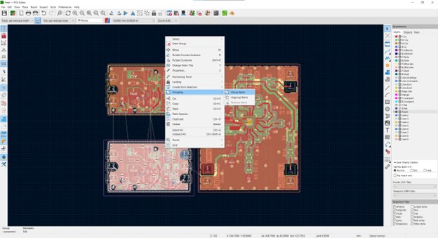
In your new KiCad project. Open the PCB editor and import each unique PCB (File->Append Board… -> *pcb*). After importing each PCB, group the entire PCB (Select All PCB Layers -> *right click* -> Grouping -> Group Items). Grouping the PCB stops you from accidentally shifting one of the layers.
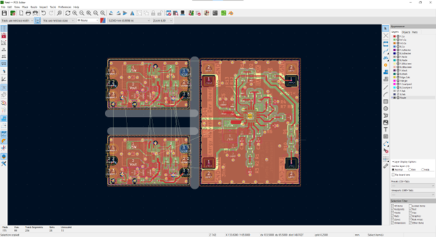
Next, you’ll want to space out the boards so that they comply with PCBWAY’s standard process. For us this means making sure boards are separated by at least 1.6mm and neighboring V score’s by at least 2mm (note I’m intentionally ignoring the PCB size requirement just for a demo).
A nice way to check the spacing is to add a route layer to your PCB. To add a route layer, go to your board stackup editor (File->Board Setup-> Board Stackup – Board Editor Layers) and rename one of the User.x layers to something like “Route”. This layer is going to be mostly just a reference, since in the end it’s the board outline that PCBWAY will care about.
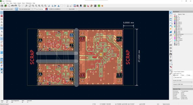
Next, we’re going to need edge rails (also called breakaway rails) on the design. See PCBWAY’s requirements (or this link). Their recommendation is 5mm edge rails. Although they support a minimum of 3mm edge rails, its best to go with whatever’s standard unless you have good reason.
I labeled my edge rails as “SCRAP” to communicate to the fab that I don't care what's done with this section of the board. If you’d rather you could also just put copper pour on the rails.
Next, these edge rails need fiducials and tooling holes for assembly. The fiducial should be between 1-3mm, with a keepout expanding 3 times that radius. There shouldn’t be anything in this keepout, soldermask, silkscreen, copper, etc. The tooling holes are less complex, they should be 2mm and are generally NPTH (non-plated through hole). Lastly where to place the tooling holes is discussed here.
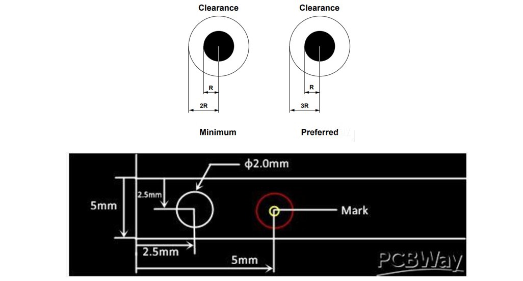
>NOTE< Creating the fiducial and tooling hole footprint is out of scope here… there’s lots of good tutorials on creating custom footprints in KiCad ;)
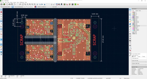
Here’s roughly how it might look afterwards. Reminder, my panel wouldn’t be accepted here since its below the minimum size for V score. This is just a demo.
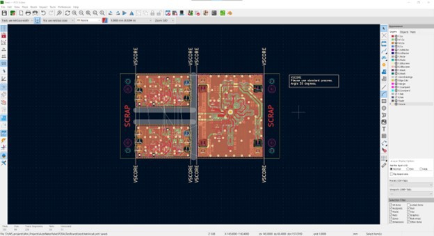
Next let’s place the V score. To do this add a V score layer, just like we did for the Route layer. On this new layer, place vertical or horizontal lines where you’d like the V score to land. (optional) You could also add a comment to this layer with any clarifications, such as the angle of the score. This comment should also be added to the order at checkout.
Almost done! Now just cleanup the panel by adding material connecting all the boards. Generally I cleanup the board outline until I’m able to view the PCB in KiCad’s 3D viewer (the 3D viewer can only accomidate one outline, so its a good sanity check).

Here's an example of a board I actually ordered.
Discussions
Become a Hackaday.io Member
Create an account to leave a comment. Already have an account? Log In.