Step-by-Step Guide for Using Breadboard++
Step 1: Install the Teensy Driver
- Go to the Teensy driver download page.
- Follow the installation instructions provided to install the Teensy driver on your computer.
Step 2: Install CoolTerm
- Download CoolTerm from this link.
- Install CoolTerm following the instructions on the website.
Step 3: Connect and Configure CoolTerm
- Open CoolTerm and select the correct COM port for the Breadboard++ device.
- Press Ctrl + T to open the terminal window for sending commands.
Command Syntax
- To connect two rows:
- Use the command format:
(row1) (row2) connect - Example:
x4 y8 connect(connects row x4 to row y8)
- Use the command format:
- To disconnect two rows:
- Use the command format:
(row1) (row2) disconnect - Example:
y8 x5 disconnect(disconnects row y8 from row x5)
- Use the command format:
- To clear all connections:
- Use the command:
clear all
- Use the command:
Step 4: Send Commands
- After typing your command in the terminal, click the Send button to execute it.
Communication
The Breadboard++ communicates with the laptop serially. You can use any terminal application to access it, but the Teensy driver needs to be installed first. I prefer using CoolTerm because it makes sending and receiving commands simple. Other terminal options include Tera Term 5 and PuTTY.
Methodology
For this project,
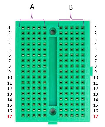
I'm using a 170-point mini prototyping breadboard, featuring 17 columns and 2 block of rows.

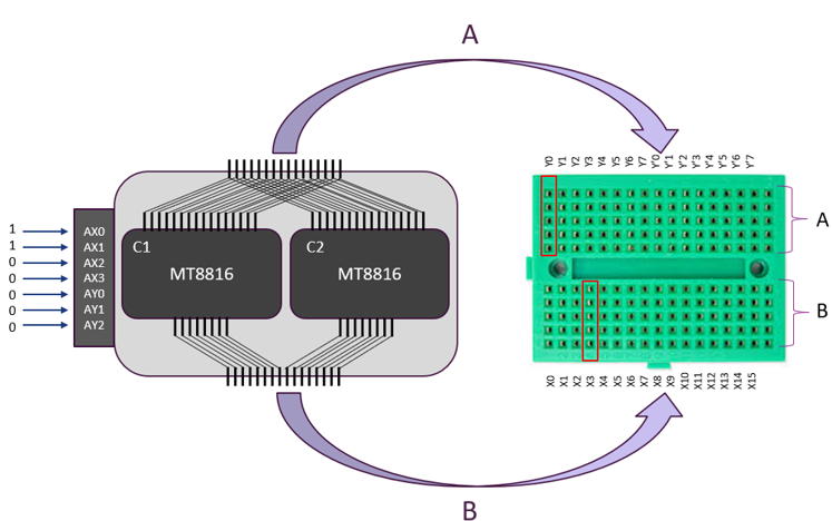
Since the cross-point array switch IC operates on a 16x8 matrix switch configuration, I combined two ICs to achieve a 16x16 matrix switch configuration
There are three types of connections that can be established on this breadboard:
Connections between each column: A -> B
Within each columns: A -> A and B -> B
So three pairs of IC’s are required
MT8816 cross-point analog array switch IC requires a 7-bit address to connect specific points in the 16x8 matrix. To generate this 7-bit address, I'm using Teensy MCU to send different addresses for connecting the points.

For instance:
To connect pin X3 to pin Y0 on IC C1, follow these steps based on the provided data sheet:
- The 7-bit address 1100000 is transmitted to the address lines, which is the address for selecting the required connection (X3 to Y0).
- Before transmitting the address, the Chip Select (CS) pin for IC C1 is set to HIGH, as pin Y0 is a column pin located on IC C1. Setting the CS pin HIGH enables the IC to respond to further instructions.
- While transmitting the address, the DATA pin is set to HIGH, signaling that the connection between X3 and Y0 should be established.
- Finally, the STROBE pin is toggled by sending a HIGH-LOW pulse. This pulse latches the connection between pin X3 and pin Y0, completing the process.
![]()
X0 – X16 are the rows of switch array of IC C1 and C2
Y0 – Y7 are the columns of switch array of IC C1
Y’0 – Y’7 are the columns of switch array of IC C2
 akash asbro