 J. Ian Lindsay
The bulk of the CPLD design has been debugged and translated into Quartus. Routing resources and logical units are 25% and 83% utilized, respectively. Good thing I've been phrasing 80-bit shift-registers as multiplexers, rather than flip-flops. I would have had to re-do them.
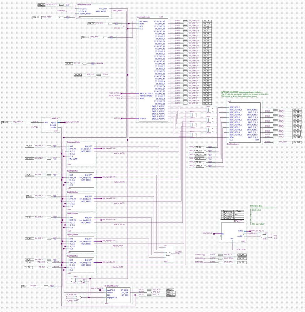
So far the following things are done:
- Clock-selection logic
- SPI address decoder, with variable post-increment chip-selection. This will allow the CPU to read all the SPI devices passively, and with a single bus-operation.
- IRQ module. This is responsible for recognizing digit-level IRQs and sending them to the CPU as an SPI bus master. It also handles the task of detecting missing digits and shutting down their electrical signals for reasons of power conservation as well as signal integrity.
- State-transistion logic for address-decoder responsible for eliminating signal skew.
- Chip-select hold-and-release logic for SPI1 interface.
- Addition of the register responsible for address bounds-checking to ensure that the bus is released prior to over-running the target address during aggregated transactions.
- Version register.
Most of what remains to be done is interconnection work within the address decoder module. This CPLD design can have an additional 95 flip-flops added to it before optimization becomes necessary. I doubt I'll need more than 28 to finish the entire TODO list. And after I convert a few core pieces into "sum-of-terms", I estimate I will achieve all design goals with at least 64 flip-flops to spare.
Onward....
Discussions
Become a Hackaday.io Member
Create an account to leave a comment. Already have an account? Log In.