 J. Ian Lindsay
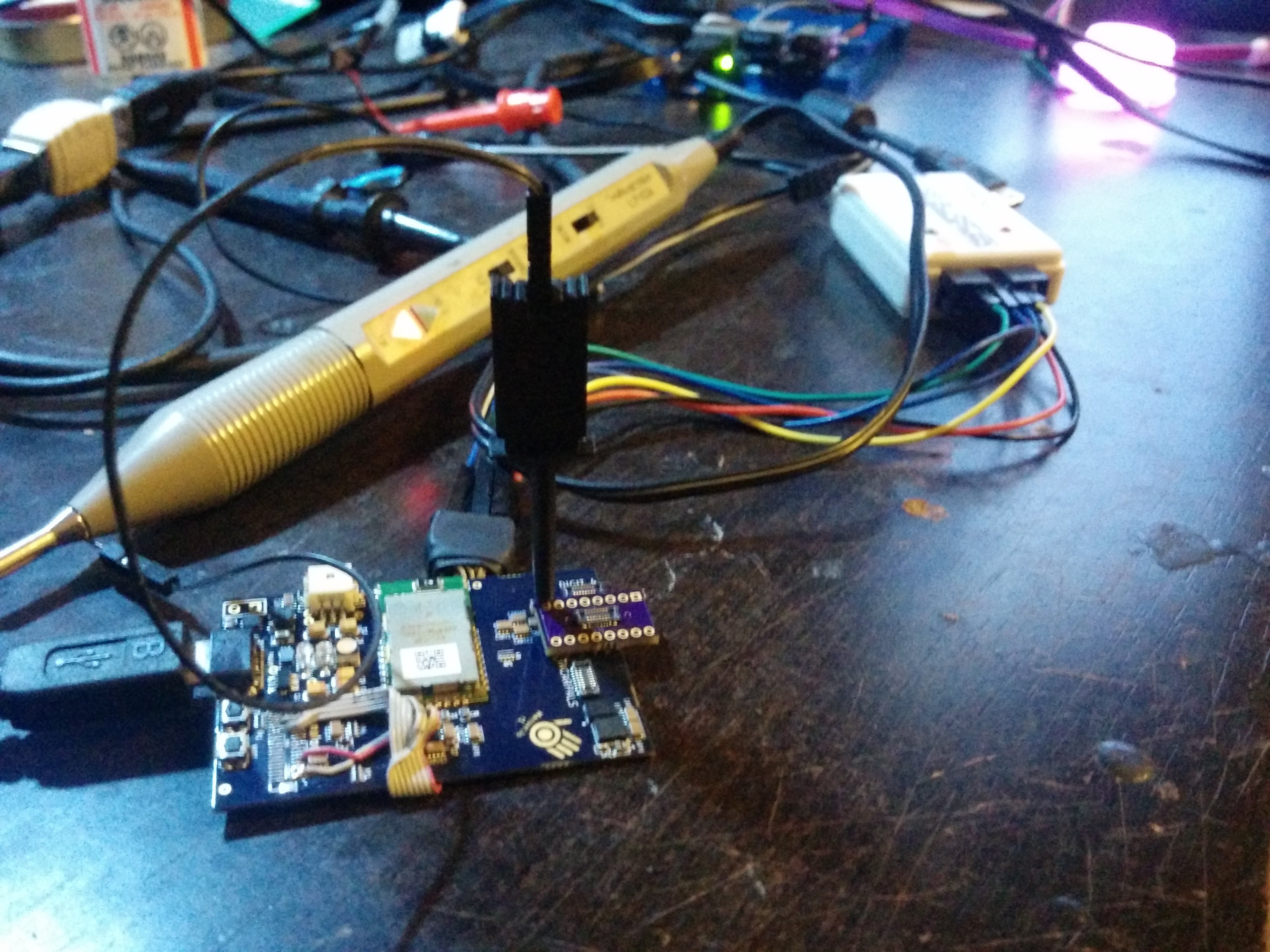
That's the r1 main board with no battery plugged into USB, a logic probe, and the JTAG dongle for the CPLD. The small purple PCB is the debug harness for the digits.
Things that work:
* Buffered clock selection (external vs internal), synchronous reset.
* Basic chip-select functionality
* Tri-state SPI1 CS logic (after some argument).
* Address demux and cycle logic
Broken things:
* IRQ aggregation state machine.
* SPI bus-master behavior is inconsistent.
* Software. Much of the infrastructure is improved, but the logical hook-up to the hardware SPI peripheral isn't there yet.
This is the part of the dev-cycle where two complex systems meet on a strand of copper wire. Getting this piece right will take some more time. But once I've finished, I can give some real-world transfer-rate benchmarks.
Onward....
Discussions
Become a Hackaday.io Member
Create an account to leave a comment. Already have an account? Log In.