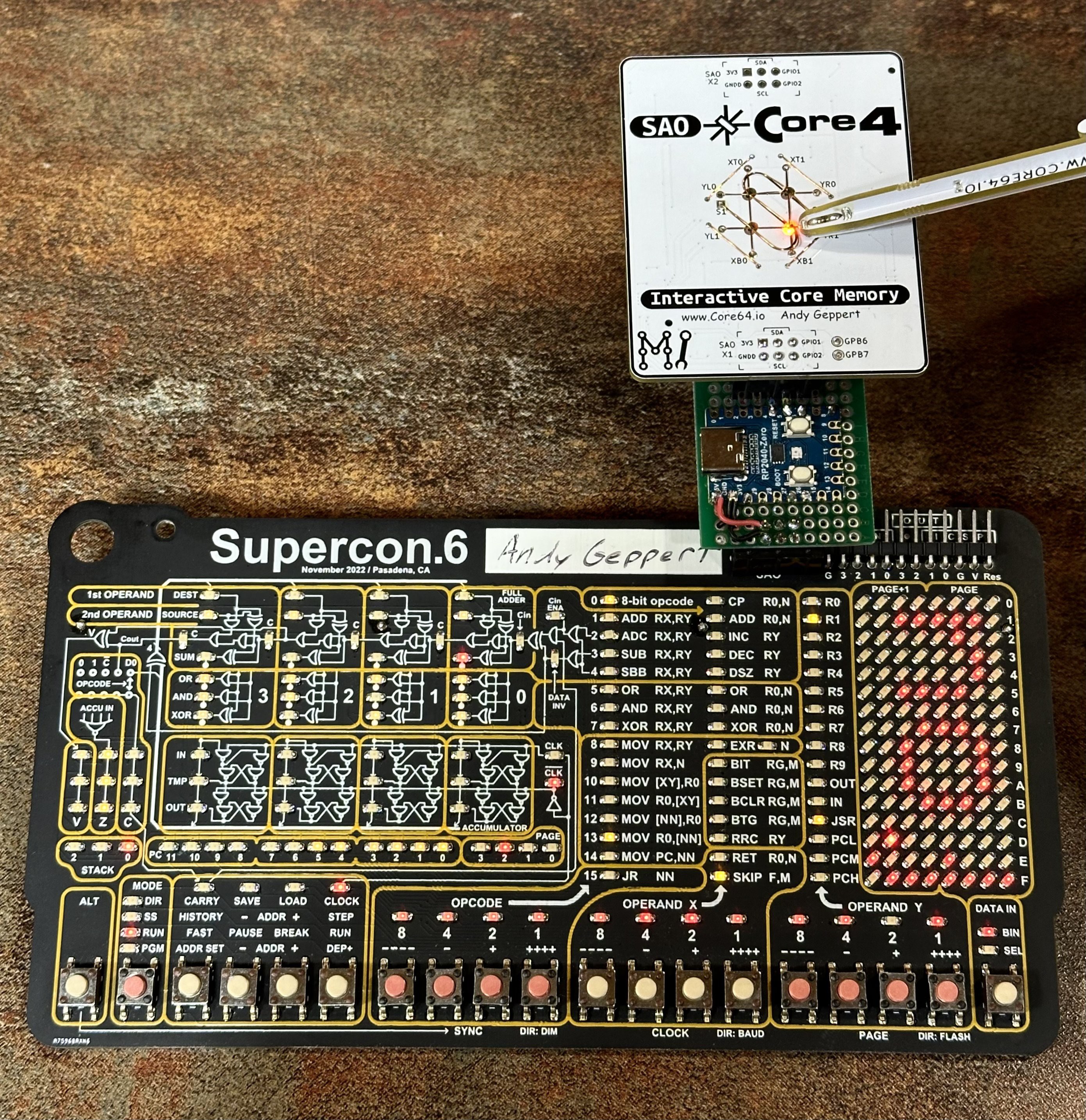
This is a break-through day of progress. All of the core functionality is working! This is the one and only mode I have right now - FLUX DETECTOR:

I've been doing this core thing for awhile, and was pleasantly surprised to find the bring-up process went smoothly. At least, from the design perspective. Had some weird issues with the Arduino IDE, but it's working fine now. And I made really dumb code comment error that sent me way off the path with some compiler messages that did not compute.
The MCU running this is an RP2040 Zero. I'm using that to see how it works, and it is a candidate for another SAO MCU project. I'm enjoying the USB-C port. I wish all the Pico boards came with that! The other MCU I'm considering is an ESP32-C3, which would open the door for Wifi and BT. Another project for later...
In the photo above, the Voja4 badge is just supplying power to the RP2040 and the Core4. I was happy to see that end of the voltage range was still able to drive the badge and the SAO.
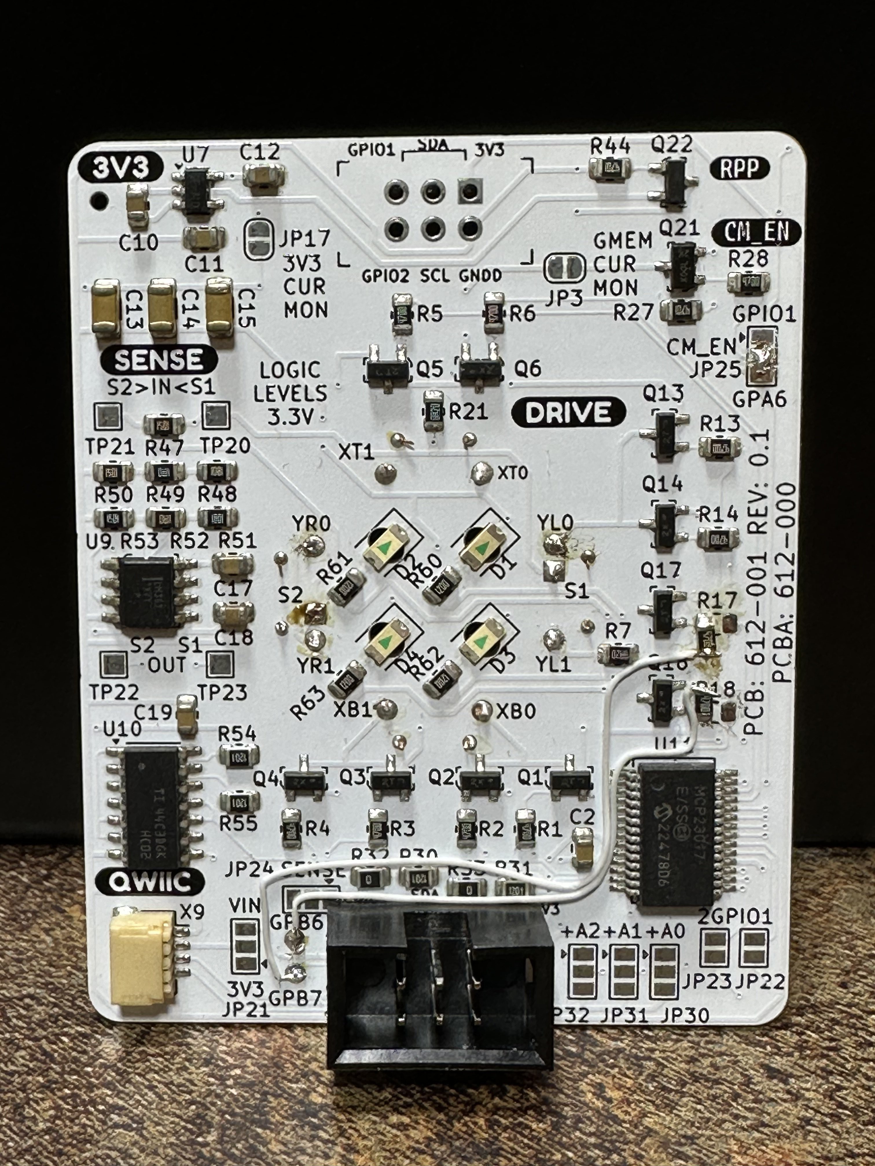
As I started to build out some documentation of the core activation process in the code, I quickly realized that a "clever" design change made understanding how the cores work more difficult. It did free up 2 GPIO pins on the IO Expander, but I decided to commit to a more straightforward electronic design, to make this easier for people to develop their own firmware with. So I've backed out that optimization, and have already started working on the next board design which strips out several features I included in the first prototypes. Most of those features were to give me flexibility to experiment and test. Now that the design is functioning, and I've chosen to simplify, I'm going to reduce the size of the board for the SAO Challenge. But, that's work for later on.
Here is what the design changes look like - relatively minor with the resistor rotations and 2 white wires:

More to come later this weekend. I think the next update will include a video of a game demo!
Meanwhile, if you have feedback on my plans for these features, let me know.
- Remove the 3V3 regulator
- Remove the 3V3 bulk storage caps
- Remove the reverse polarity protection FET
- Remove several optional solder jumpers which allow pin usage changes
- Remove the QWIIC port
- Remove the top (2nd) SAO pass-through port.
- Keep the IO Expander address setting jumpers, perhaps make them smaller.
- I'm only using GPIO2 of the SAO. GPIO1 remains open for other use. Yah know, a button would be nice to change modes... Hmmmm...
 Andy Geppert
Discussions
Become a Hackaday.io Member
Create an account to leave a comment. Already have an account? Log In.