 Marius Taciuc
-
10000 NOP instruction detailed description
0.Initial state
-the data bus is selected on read mode to all the blocks and the bus lines are LO
-the SIO are in undefined states
-The exec pulse is not present1.M_clk1 (PC pulse) increments the PC counter and modifies the address of the ROM to the new line
-the memory puts the NOP (0000) on the instruction bus and the afferent data word (XXXXXXXX) on the data bus
-the instruction decoder enables the line no 1
-line 1 is not connected
2.M_clk2 -
3.M_clk3 (Exec pulse) does nothing because all the logical AND gates having this line as an input, are having the other lines LO
4.M_clk4 deactivates (by reset) the R/W lines and all the blocks on the bus are in read mode. -
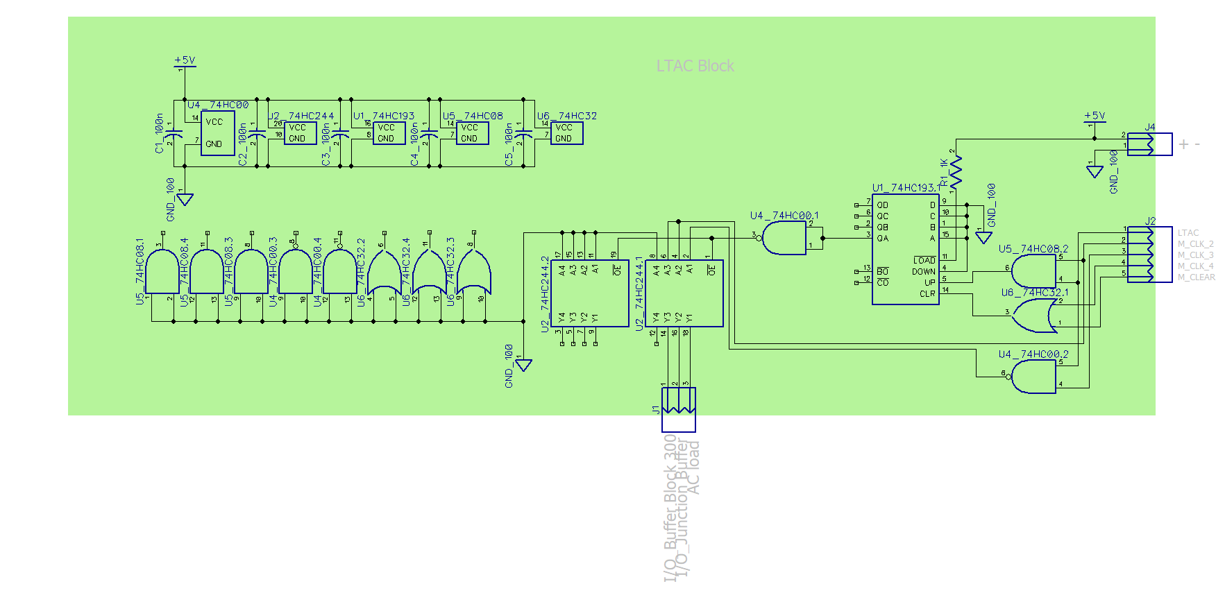
20001 LTAC
0.Initial state
-the data bus is selected on read mode to all the blocks and the bus lines are LO
-the SIO are in undefined states
-The exec pulses are not present1.M_clk1 (PC pulse) increments the PC counter and modifies the address of the ROM to the new line
-the memory puts the LTAC (0001) on the instruction bus and the afferent data word on the data bus before the I/O buffer of the 300 Block
-the instruction decoder enables the line no 2 of the SIO
-line 2 activates two logical and gates at the Enable of the I/O buffer at the output of the Block 300 and at the Enable of the I/O buffer junction
-line 2 also goes into an AND logical gate connected on the parallel load of the AC
2.M_clk2 swithces the I/O junction buffer and the block 300 I/O buffer on through the logical AND gates
3.M_clk3 (Exec pulse)enables the parallel load on AC opening the AND gate
4.M_clk4 deactivates (by reset) the I/O buffer lines and all the blocks on the bus are in read mode.
-this pulse also switches off the I/O junction buffer![]()
-
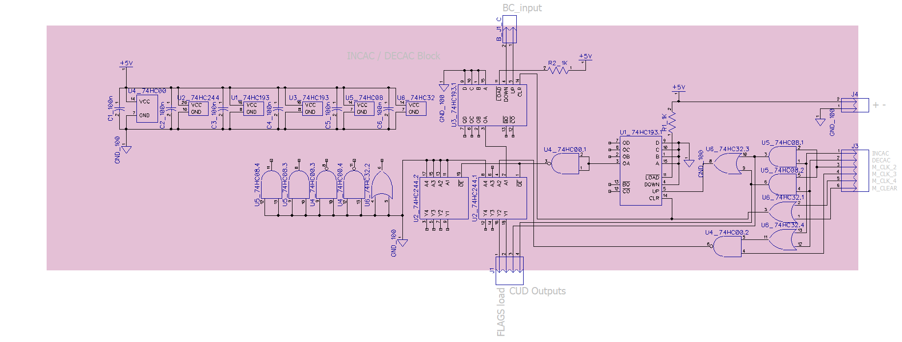
30100 INCAC and 0101 DECAC blocks
0.Initial state
-the data bus is selected on read mode to all the blocks and the bus lines are LO
-the SIO are in undefined states
-The exec pulse is not present1.M_clk1 (PC pulse) increments the PC counter and modifies the address of the ROM to the new line
-the memory puts the INCAC (0100) on the instruction bus
-the instruction decoder enables the line no 5
-the junction buffer before the AC and the I/O buffer at block 300 are deactivated by default
2.M_clk2 (Exec pulse) puts the increment pulse on the AC register and opens the I/O output buffer of the Carry flag
-the AC increments
-if the CO output of the AC gives a pulse, the Carry I/O buffer will latch HI
3.M_clk3 (Exec pulse) enables the parallel load on the FLAGS register and this will store the C or Z present flags
4.M_clk4 deactivates (by reset) the I/O buffers and all the blocks on the bus are in read mode.![]()
0.Initial state
-the data bus is selected on read mode to all the blocks and the bus lines are LO
-the SIO are in undefined states
-The exec pulse is not present1.M_clk1 (PC pulse) increments the PC counter and modifies the address of the ROM to the new line
-the memory puts the DECAC (0101) on the instruction bus
-the instruction decoder enables the line no 6
-the junction buffer before the AC and the I/O buffer at block 300 are deactivated by default
2.M_clk2 (Exec pulse) puts the decrement pulse on the AC register and opens the I/O output buffer of the Carry flag
-the AC decrements
-if the BO output of the AC gives a pulse, the Carry I/O buffer will latch HI
3.M_clk3 (Exec pulse) enables the parallel load on the FLAGS register and this will store the C or Z present flags
4.M_clk4 deactivates (by reset) the I/O buffers and all the blocks on the bus are in read mode. -
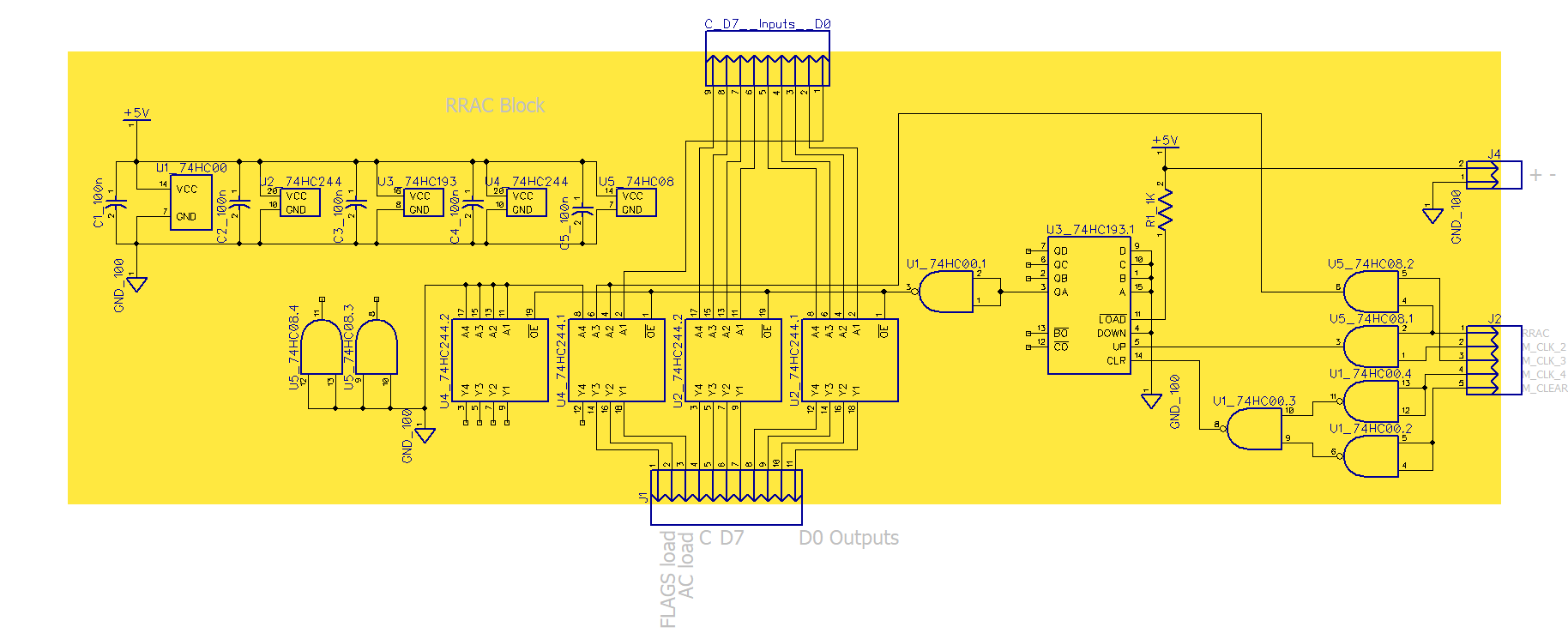
40110 RRAC and 0111 RLAC block
0.Initial state
-the data bus is selected on read mode to all the blocks and the bus lines are LO
-the SIO are in undefined states
-The exec pulse is not present1.M_clk1 (PC pulse) increments the PC counter and modifies the address of the ROM to the new line
-the memory puts the RRAC (0110) on the instruction bus
-the instruction decoder enables the line no 7
-the junction buffer before the AC and the I/O buffer at block 300 are deactivated by default
-the RRAC module is already loaded with the value of the AC
2.M_clk2 (Exec pulse) puts the rotation result on the input of the AC
3.M_clk3 (Exec pulse) enables the parallel load on the AC through an AND gate and the AC and the FLAGS are storing the result
4.M_clk4 deactivates (by reset) the I/O buffers and all the blocks on the bus are in read mode.![]()
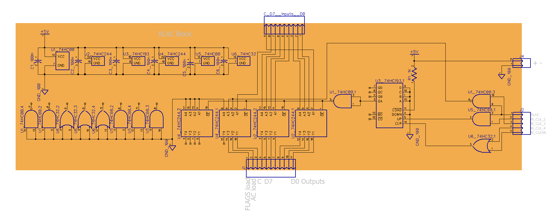
0.Initial state
-the data bus is selected on read mode to all the blocks and the bus lines are LO
-the SIO are in undefined states
-The exec pulse is not present1.M_clk1 (PC pulse) increments the PC counter and modifies the address of the ROM to the new line
-the memory puts the RLAC (0111) on the instruction bus
-the instruction decoder enables the line no 8
-the junction buffer before the AC and the I/O buffer at block 300 are deactivated by default
-the RLAC module is already loaded with the value of the AC
2.M_clk2 (Exec pulse) puts the rotation result on the input of the AC by activating the I/O buffer at the output of the RLAC block
3.M_clk3 (Exec pulse) enables the parallel load on the AC through an AND gate and the AC and the FLAGS are storing the result
4.M_clk4 deactivates (by reset) the I/O buffers and all the blocks on the bus are in read mode.![]()
-
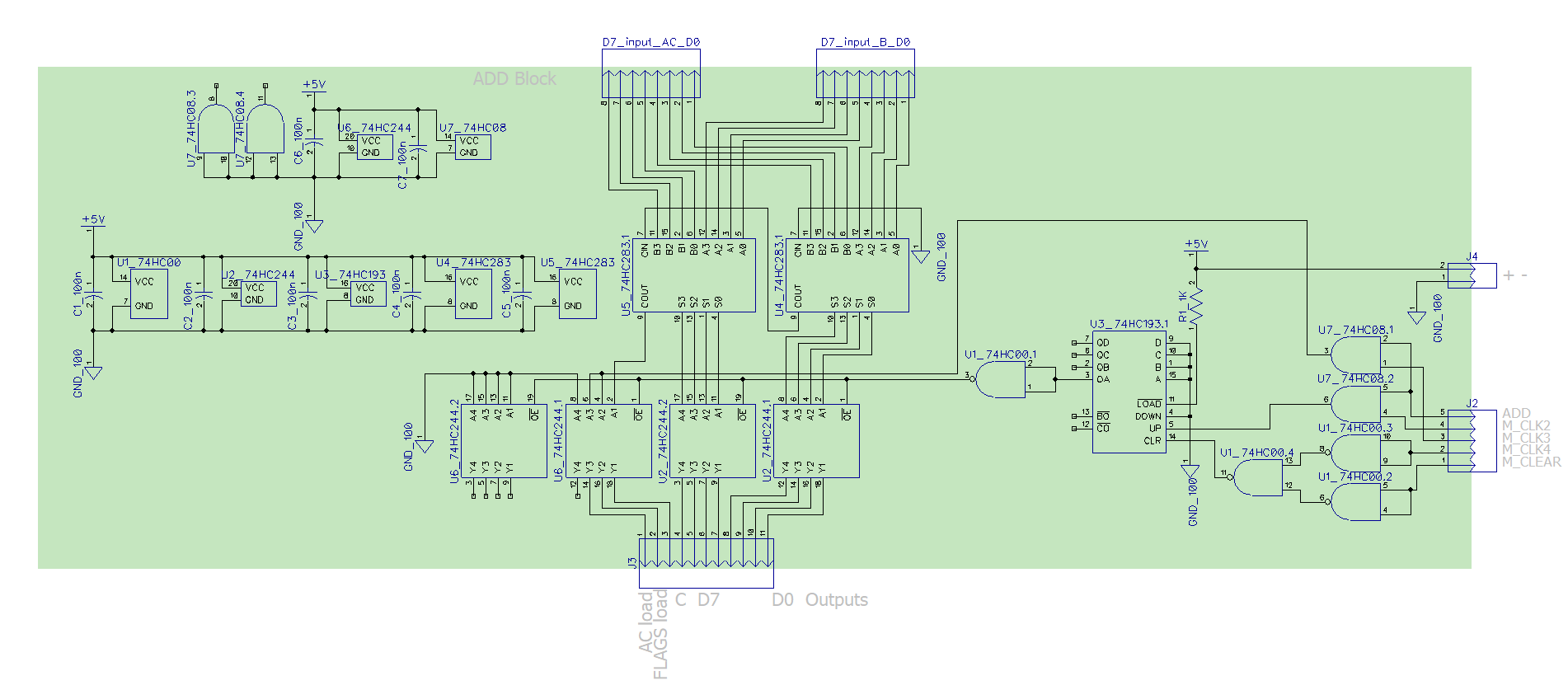
51000 ADD instruction block description
0.Initial state
-the data bus is selected on read mode to all the blocks and the bus lines are LO
-the SIO are in undefined states
-The exec pulse is not present1.M_clk1 (PC pulse) increments the PC counter and modifies the address of the ROM to the new line
-the memory puts the ADD (1000) on the instruction bus and the afferent data word (the number B) at the input of the 300 I/O buffer
-the instruction decoder enables the line no 9
-the junction buffer before the AC is deactivated by default
-the number A is found at the output of the AC before the buffer
2.M_clk2 (Exec pulse) activates the I/O buffer of the Block 300 and outputs the number B to the bus
-the pulse also enables the output I/O buffer for this ADD operation block
-This puts the result on the input of the AC
3.M_clk3 (Exec pulse) enables the parallel load on the AC and FLAGS through an AND gate and the AC stores the result
4.M_clk4 deactivates (by reset) the I/O buffers and all the blocks on the bus are in read mode again.![]()
-
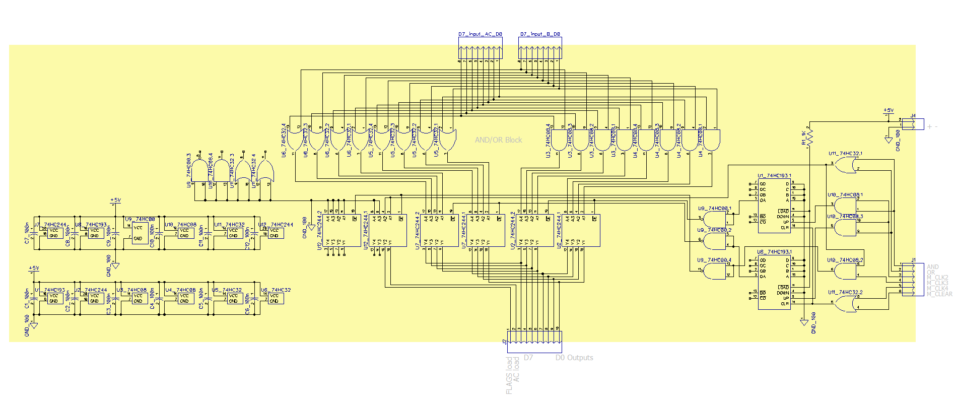
61001 OR block and 1010 AND block description
0.Initial state
-the data bus is selected on read mode to all the blocks and the bus lines are LO
-the SIO are in undefined states
-The exec pulse is not present1.M_clk1 (PC pulse) increments the PC counter and modifies the address of the ROM to the new line
-the memory puts the OR (1001) on the instruction bus and the afferent data word (the number B) at the input of the 300 I/O buffer
-the instruction decoder enables the line no 10
-the junction buffer before the AC is deactivated by default
-the number A is found at the output of the AC before the buffer
2.M_clk2 (Exec pulse) enables the output I/O buffer for this OR operation block
-This puts the result on the input of the AC
-the pulse also activates the buffer I/O buffer of the Block 300 and outputs the number B to the bus
3.M_clk3 (Exec pulse) enables the parallel load on the AC through an AND gate and the AC stores the result
4.M_clk4 deactivates (by reset) the I/O buffers and all the blocks on the bus are in read mode.
![]()
0.Initial state
-the data bus is selected on read mode to all the blocks and the bus lines are LO
-the SIO are in undefined states
-The exec pulse is not present1.M_clk1 (PC pulse) increments the PC counter and modifies the address of the ROM to the new line
-the memory puts the AND (1010) on the instruction bus and the afferent data word (the number B) at the input of the 300 I/O buffer
-the instruction decoder enables the line no 11
-the junction buffer before the AC is deactivated by default
-the number A is found at the output of the AC before the buffer
2.M_clk2 (Exec pulse) activates the I/O buffer of the Block 300 and outputs the number B to the bus
-the pulse also enables the output I/O buffer for this AND operation block
-This puts the result on the input of the AC
3.M_clk3 (Exec pulse) enables the parallel load on the AC through an AND gate and the AC stores the result
4.M_clk4 deactivates (by reset) the I/O buffers and all the blocks on the bus are in read mode again. -
71011 JTO (Jump to) instruction description
0.Initial state
-the data bus is selected on read mode to all the blocks and the bus lines are LO
-the SIO are in undefined states
-The exec pulses are not present1.M_clk1 (PC pulse) increments the PC counter and modifies the address of the ROM to the new line
-the memory puts the JTO (1011) on the instruction bus and the afferent data word (the new PC) on the data bus
-the instruction decoder enables the line no 12
-line 12 activates R/W PC line of the block 300 wich goes into a logical AND gate inside the block
2.M_clk2 -
3.M_clk3 (Exec pulse)enables the parallel load on PC through a logical AND gate (connected on R/W PC)
4.M_clk4 deactivates (by reset) the I/O buffer lines and all the blocks on the bus are in read mode.!Atention! the next pulse cycle will increment the PC again with M_clck1.
If you want to reach a certain instruction in the ROM, think of it as PC-1 -
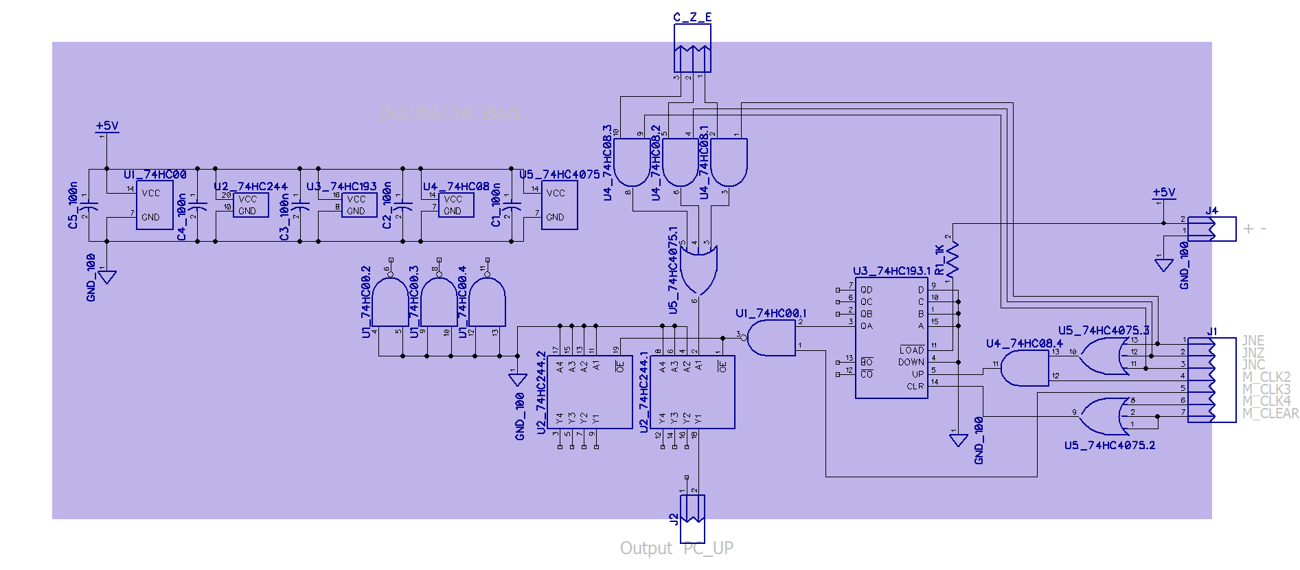
81100, 1101 and 1110, JNZ, JNE and JNC instructions description
These 3 instructions come in a single block and their description matches the order in the title.
0.Initial state
-the data bus is selected on read mode to all the blocks and the bus lines are LO
-the SIO are in undefined states
-The exec pulse is not present1.M_clk1 (PC pulse) increments the PC counter and modifies the address of the ROM to the new line
-the memory puts the JNZ (1100) on the instruction bus
-the instruction decoder enables the line no 13
-the junction buffer before the AC and the I/O buffer at block 300 are deactivated by default
-the JUMP block module is already loaded with the value of the FLAGS
2.M_clk2 (Exec pulse) activates the I/O buffer at the output of the JUMP module
3.M_clk3 (Exec pulse) outputs a pulse that will increment the PC only if the speciffic flag is present
4.M_clk4 deactivates (by reset) the I/O buffers and all the blocks on the bus are in read mode.0.Initial state
-the data bus is selected on read mode to all the blocks and the bus lines are LO
-the SIO are in undefined states
-The exec pulse is not present1.M_clk1 (PC pulse) increments the PC counter and modifies the address of the ROM to the new line
-the memory puts the JNE (1101) on the instruction bus
-the instruction decoder enables the line no 14
-the junction buffer before the AC and the I/O buffer at block 300 are deactivated by default
-the JUMP block module is already loaded with the value of the FLAGS
2.M_clk2 (Exec pulse) activates the I/O buffer at the output of the JUMP module
3.M_clk3 (Exec pulse) outputs a pulse that will increment the PC only if the speciffic flag is present
4.M_clk4 deactivates (by reset) the I/O buffers and all the blocks on the bus are in read mode.0.Initial state
-the data bus is selected on read mode to all the blocks and the bus lines are LO
-the SIO are in undefined states
-The exec pulse is not present1.M_clk1 (PC pulse) increments the PC counter and modifies the address of the ROM to the new line
-the memory puts the JNC (1110) on the instruction bus
-the instruction decoder enables the line no 15
-the junction buffer before the AC and the I/O buffer at block 300 are deactivated by default
-the JUMP block module is already loaded with the value of the FLAGS
2.M_clk2 (Exec pulse) activates the I/O buffer at the output of the JUMP module
3.M_clk3 (Exec pulse) outputs a pulse that will increment the PC only if the speciffic flag is present
4.M_clk4 deactivates (by reset) the I/O buffers and all the blocks on the bus are in read mode.![]()
-
9Other functional blocks that go into the main schematic
E detect block.
Used for the E (equal) flag. Activates the particular line when the two numbers are identical.
![]()
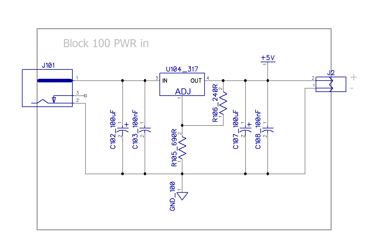
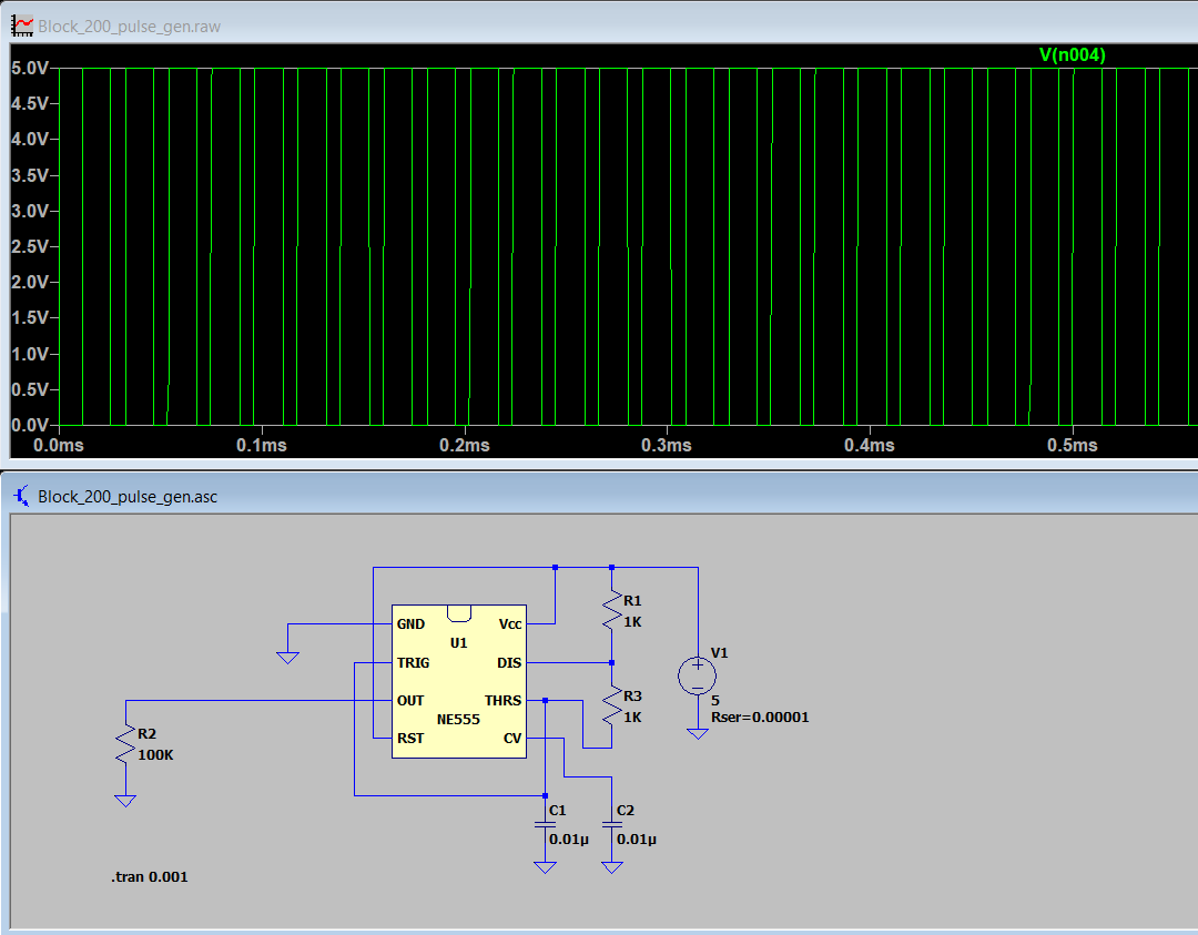
PWR generating clock,
is basically used for powering the entire computer:
![]()
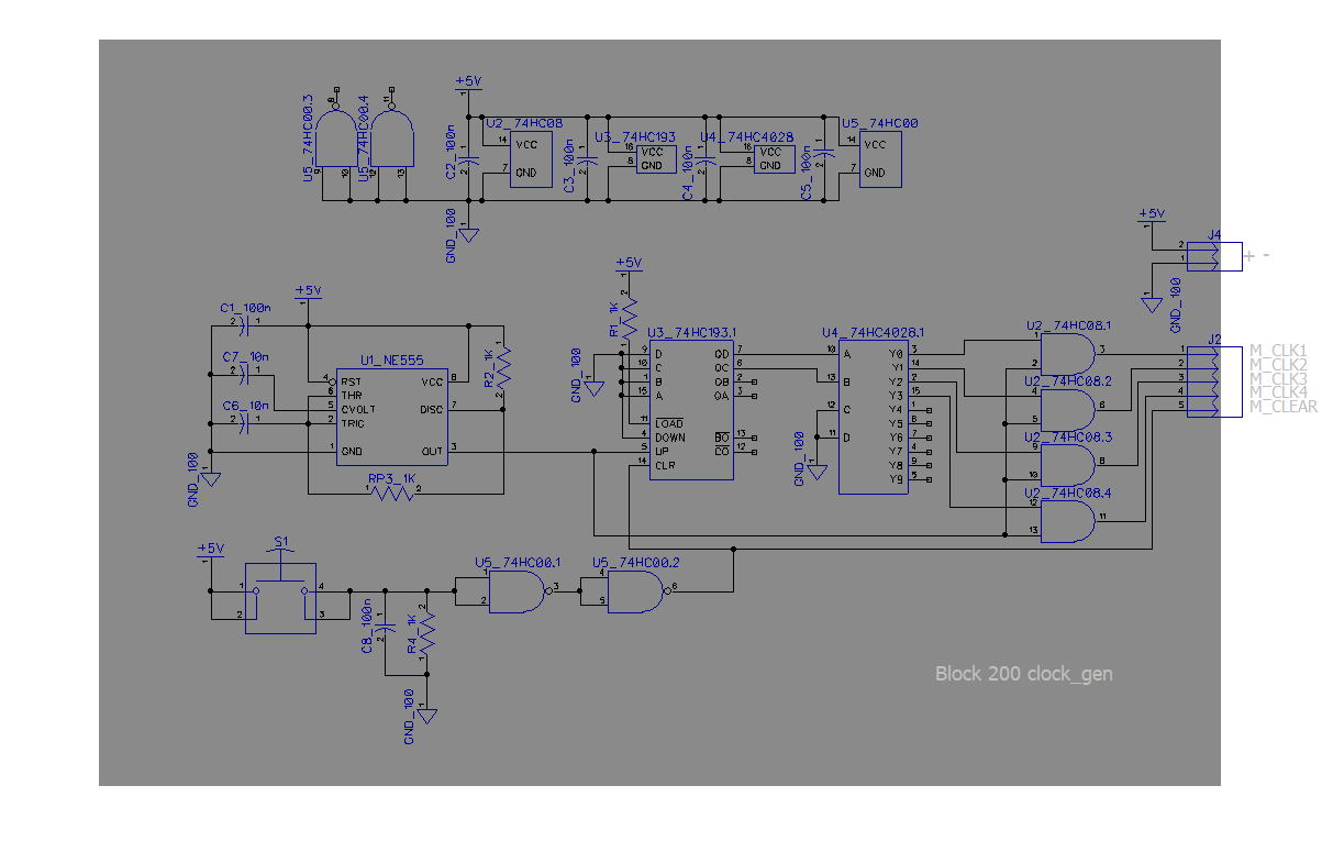
Clock generating module:
![]()
![]()
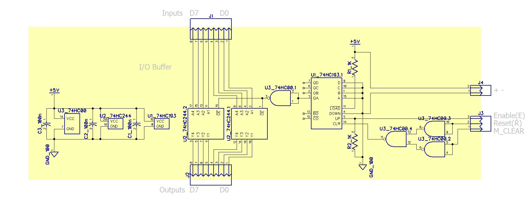
IO buffer block
It is used as a separation gateway for connecting to the bus. In order to avoid having 2 different blocks talking to he same bus, the unused buses can be disconnected through these serial switches.
![]()
-
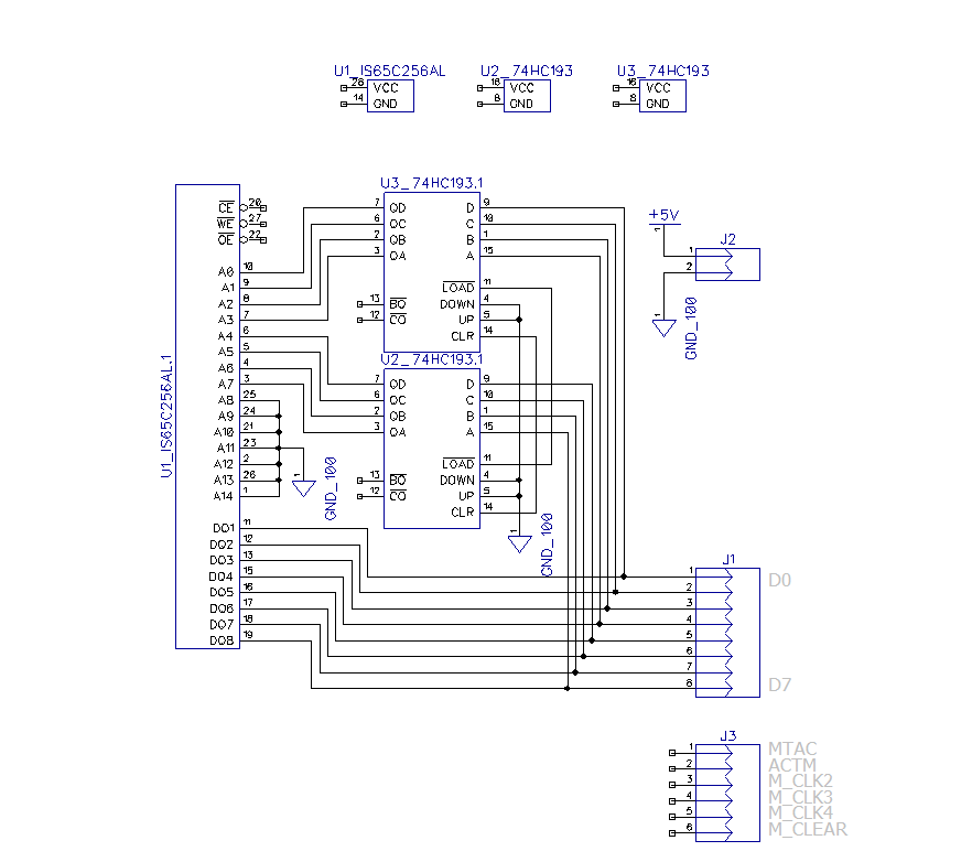
10RAM and output port module
This module is not finished yet. The idea would be to have a RAM memory or a stack or register chips working together as a volatile memory. The last address in the memory would be connected to 8 external LEDs and pins. This can be used as the output IO port of a regular microcontroller.
![]()
B4 Thinker - 4 bit homebrewed computer
Scratch built architecture of a CPU and some of its peripherals.
Discussions
Become a Hackaday.io Member
Create an account to leave a comment. Already have an account? Log In.