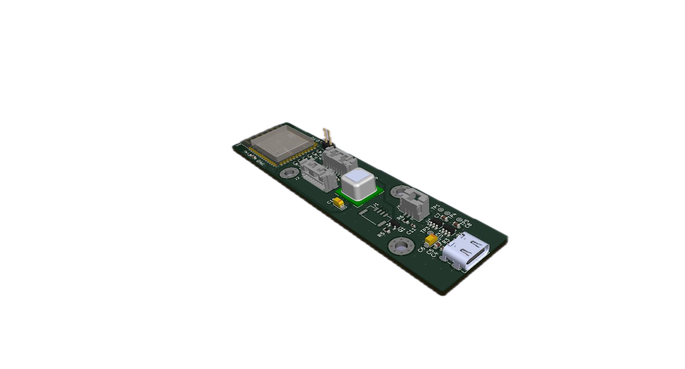
Once I selected the appropriate processor and sensors, it was onto the PCB design

Designing the printed circuit board (PCB) for my smart hive project was an intricate and rewarding process, and it wasn’t something I tackled alone. Recognizing the complexity involved, I decided to collaborate with a talented university student who brought fresh insights and technical skills to the table. Together, we worked on laying out and designing the PCB, ensuring it would meet all the specific needs of my IoT beekeeping system.
The PCB serves as the central hub where all the electronic components connect, making it essential to get the design just right. We had to carefully consider the physical constraints of "bee space" and ensure that the board was compact yet efficient, fitting seamlessly into the hive without disrupting the bees. Additionally, the layout needed to optimize power efficiency and signal integrity while minimizing noise, crucial factors for maintaining accurate data transmission from the various sensors.
The collaborative effort allowed us to combine practical engineering with innovative design, resulting in a PCB that not only functions perfectly but is also easy to assemble and integrate into the hive. This experience underscored the value of merging academic knowledge with hands-on experience, leading to a design that will serve as the foundation for the ongoing development of my smart hive prototype.
You can view details of the board, components and wiring in 'Files.'
 Kevin Jablonski
Discussions
Become a Hackaday.io Member
Create an account to leave a comment. Already have an account? Log In.