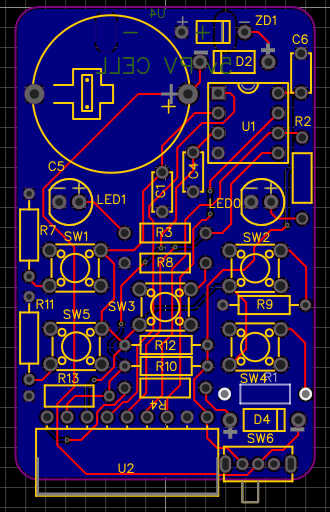
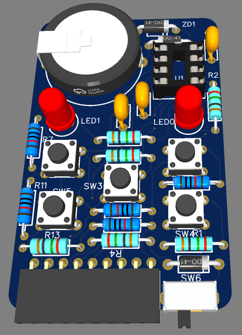
The PCB I am designing on EasyEDA is almost complete. I decided to go with all through hole components. Mainly for ease of soldering, and most people doing a DIY project might prefer the through hole soldering ;)... Also there is some thing about the beauty of these components vs. SMD.
Below are some screenshots of the schematic, PCB, and 3d view. For this design, my idea was to make the PCB somewhat smaller than the inside of the tic-tac box, and 3d printing a frame that the components can mount to, then the entire assembly can slide into be box no problem. The Solar cell will get wires soldered to it, then it will mount on one side of the frame, and the wires will be soldered to pads on back of the PCB.
Some changes of this design vs the protoboard prototype I have made:
- Changed the VCC voltage divider resistors on ADC2 to a 3.9Mohm & 1Mohm, and added a 100nF capacitor. I need to test this in real life to see if this will give accurate enough readings.
- Removed the 3 pin header on top of device in favor of only having 1 pin header.
- "Tried" to find tactile switches that are just the right height, in order to be able to press the switches through the tic-tac box, eliminating the need to drill or cut any holes in the box whatsoever. I am not sure if this will work, but the box is pretty flexible, and if the switch plungers are tight with the inside of the box, I imagine it will work.
- Also chose a slightly thinner supercapacitor style with the same capacitance and voltage rating.
- Added a 20ohm resistor on VIN, incase capacitor is fully discharged. This is to prevent a huge current draw while programming it from Arduino. I have not experienced this, but I have heard that if the capacitor is depleted, it can try to draw over an amp or more of current initially. We don't want to burn out a voltage regulator or USB port.
- Added 100nf capacitor on Button ADC3 pin. This is also another contingency incase readings are not stable. I have not found the need for this on the prototype, but the holes are there incase it is needed.
I have been looking at this design, and realizing this would be a good candidate for encasing the entire device in clear resin, pouring it just high enough as to not glue the buttons plungers in position. I have seen some people do similar things with similar devices on youtube...
Also just a 3d printed case would also work good for this device, but for now, the tic-tac box works great. I do not have access to a 3d printer.


 Gordon
Discussions
Become a Hackaday.io Member
Create an account to leave a comment. Already have an account? Log In.