Two posts ago our CPU was demonstrated connected to an Arduino to provided memory-mapped I/O. This MMIO space could hold code, other board-level I/O functions or perform functions on the host PC. The 'memory' area of this MMIO space was slow - each access had to be interpretted by code running on the Arduino.
In the next post the Arduino was taken away and replaced with memory that went as fast as the bus could drive it! But it had no I/O and no code to run on it.
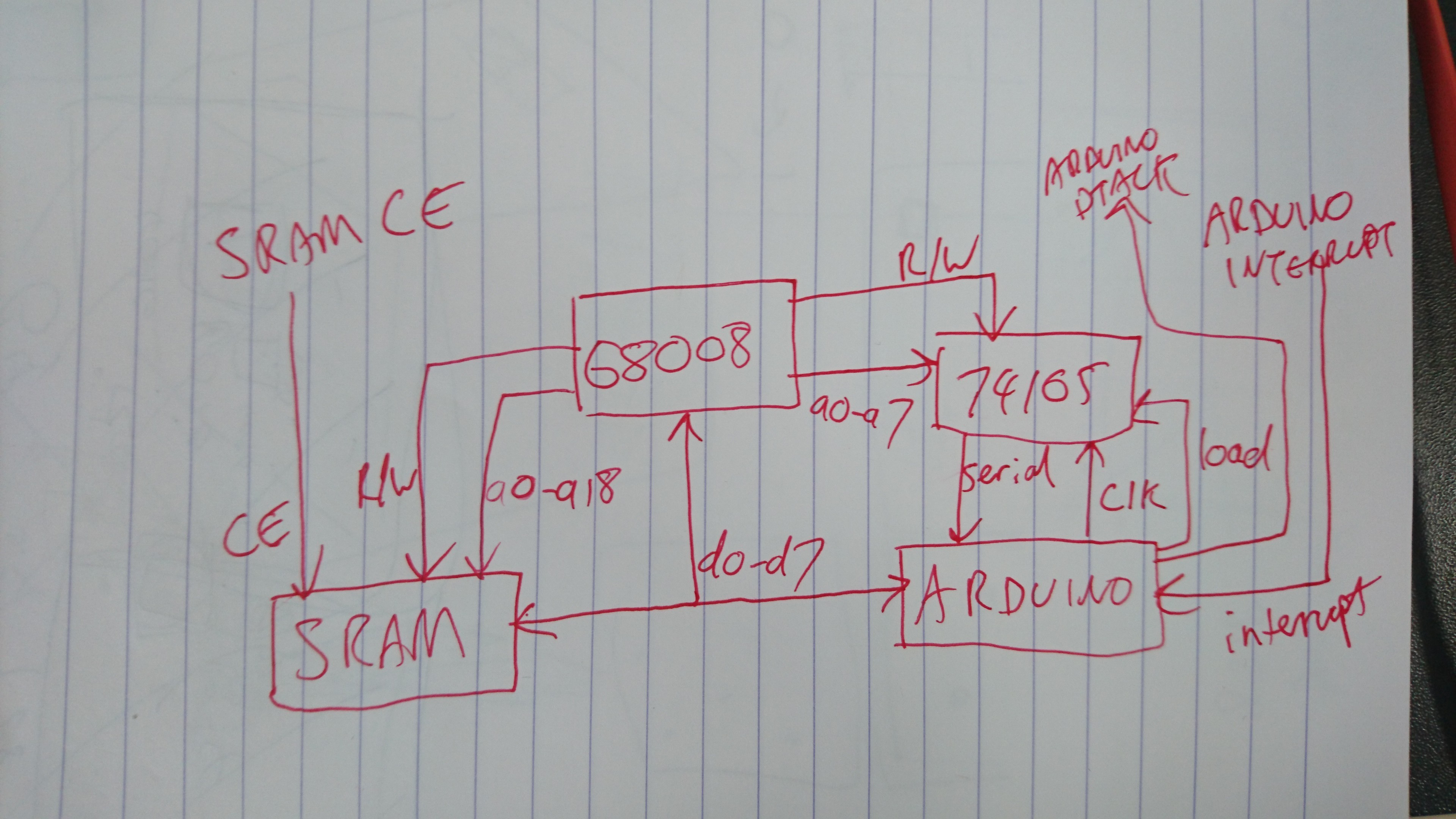
Let's combine the two. This is pretty easy. To recap the signals required for each device. The changes we need to make are highlighted in bold.
SRAM
- write-enable (WE) is connected directly to the CPU's R/W signal
- output-enable (OE) is tied low
- chip-enable (CE) was tied to the CPU's (address strobe) AS signal, to activate the read/write operation when all the inputs are ready. The CPU's AS signal will assert regardless of the address chosen. We need to restrict this CE signal to be only when the addresses we are interested in are in use
- the 8-bit data bus is connected directly to both the CPU and SRAM. When the CE is not asserted the RAM's inputs will go into a high impedance state, allowing other devices on the same bus to drive a signal.
- the 19-bit RAM address bus is connected to the CPU's A0-A18 address bus, continuing to leave A19 unused by the RAM.
- the CPU has its DTACK signal grounded when the RAM is in use, to indicate no wait states. The RAM is fast enough to satisfy the CPU.
Arduino
- the CPU's R/W signal and a number of address lines are connected to a 74'165 shift parallel-in serial-out shift register. When the Arduino wants to read one of these signals, it captures them all in the register then shifts them in one at a time.
- the 8-bit data bus is connected directly to eight of the Arduino's digital data pins. When the Arduino is not in use, these pins are in a high impedance state allowing another device to command the data bus.
- the Arduino's interrupt pin was tied to the CPU's AS signal, to activate the read/write operation when all the inputs are ready. The CPU's AS signal will assert regardless of the address chosen. We need to restrict this signal to be only when the addresses we are interested in are in use
- when the Arduino is in use, the CPU has its DTACK signal connected to an output from the Arduino. It holds it high until the operation is processes, then grounds it for one clock cycle.
Address decoding
So the set-up of two devices is pretty similar. We really only need to do two things - send AS to the right place and receive DTACK from the right place. This place will depend on which address is on the address bus.
In the previous post, as only A0-A18 were connected to the RAM and A19 was left free this turned our 1 MB address space into two 512 KB mirrors of the same RAM. If for instance we only triggered the RAM's chip enable with AS when A19 was low - ie the low 512 KB of the address space - the upper 512 KB could be used for something else. Or vice versa - if the AS signal triggered CE when A19=1 then the 512 KB RAM would appear in the top 512 KB of the address space and the bottom 512 KB would be undefined. There would be no data on the bus and the CPU would read junk.
The same thing applies to the Arduino. Suppose on our shift register we shift in the CPU R/W signal and eight bits of address (A0-A7), if the Arduino interrupt was triggered on every AS then the Arduino address space would mirror every 256 bytes from address zero to the top address: 1 MB. If this signal was only triggered when A19=0 then the Arduino MMIO space would only exist from address zero to the middle of the address space - 512 KB in. The top 512 KB would be undefined.
With a tiny bit of logic we can make ourselves some address decoding. Let's map the Arduino into 256 byte mirrors in the bottom 512 KB and the 512 KB SRAM into the top 512 KB.
Here's a truth table for the chip selects. Remember that AS and the two chip enables are active low.
| CPU /AS | CPU A19 | SRAM /CE | Arduino /interrupt |
| 0 | 0 | 1 | 0 |
| 0 | 1 | 0 | 1 |
| 1 | 0 | 1 | 1 |
| 1 | 1 | 1 | 1 |
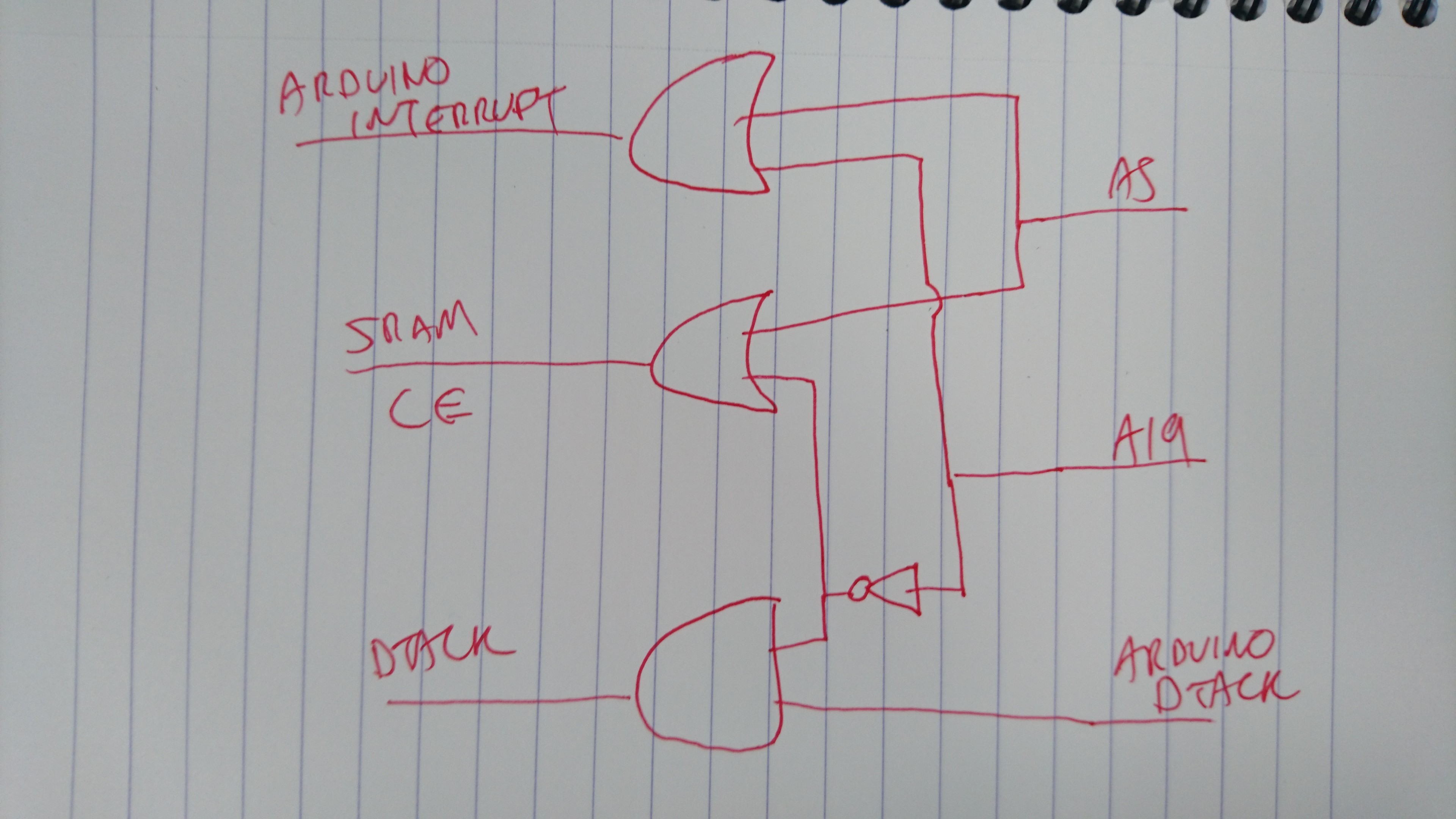
Using this solver we can make ourselves some logical equation for this.
and a truth table for the /DTACK signal that goes to the CPU. Also active low.
| CPU A19 | Arduino /DTACK | CPU DTACK |
| 0 | 0 | 0 |
| 0 | 1 | 1 |
| 1 | 0 | 0 |
| 1 | 1 | 0 |
/DTACK = !A19 && /ARDUINO_DTACK
Adding some gates
In order to implement our three equations we will need some logic gates. We could just use NAND or NOR gates but perhaps let's just use the logical operations described by the equations above: NOT, OR and AND.
For NOT I'm going to use a 74'04 - six NOT gates in one package.
For AND I'm going to use a 74'08 - four two-input AND gates
For OR I'm going to use a 74'32 - four two-input OR gates.
So far I've been using the "HC" variants of these chips. Compatible with TTL logic, can use a ~5V power supply and reasonably fast switching times. Mine are all from Texas Instruments.
Schematics
Wire this up. This is the CPU, SRAM and Arduino connection (along with the Arduino's shift register).

And here's the logic to wire up too. This implements the three equations described above.
Conclusion
At this point you have a CPU with 512 KB of fast working memory, in addition to an Arduino which can perform any I/O that you want. It can also supply code - replacing a ROM or other file store. The address space looks like this:
- 0x00000-0x000FF - the Arduino MMIO area
- mirrors of this region up to 0x80000
- 0x80000-0xFFFFF - 512 KB of zero wait state static RAM
At this point some may notice I have not described how to reset the circuit...to do this reliably is more complex than you might imagine but that will be for another day!

Discussions
Become a Hackaday.io Member
Create an account to leave a comment. Already have an account? Log In.