 deʃhipu
So the "fixed" PCBs arrived. This time I didn't order assembly, just the PCBs, so I simply transplanted all the parts from one of the first prototype boards to the new one. Connected it, and voila:
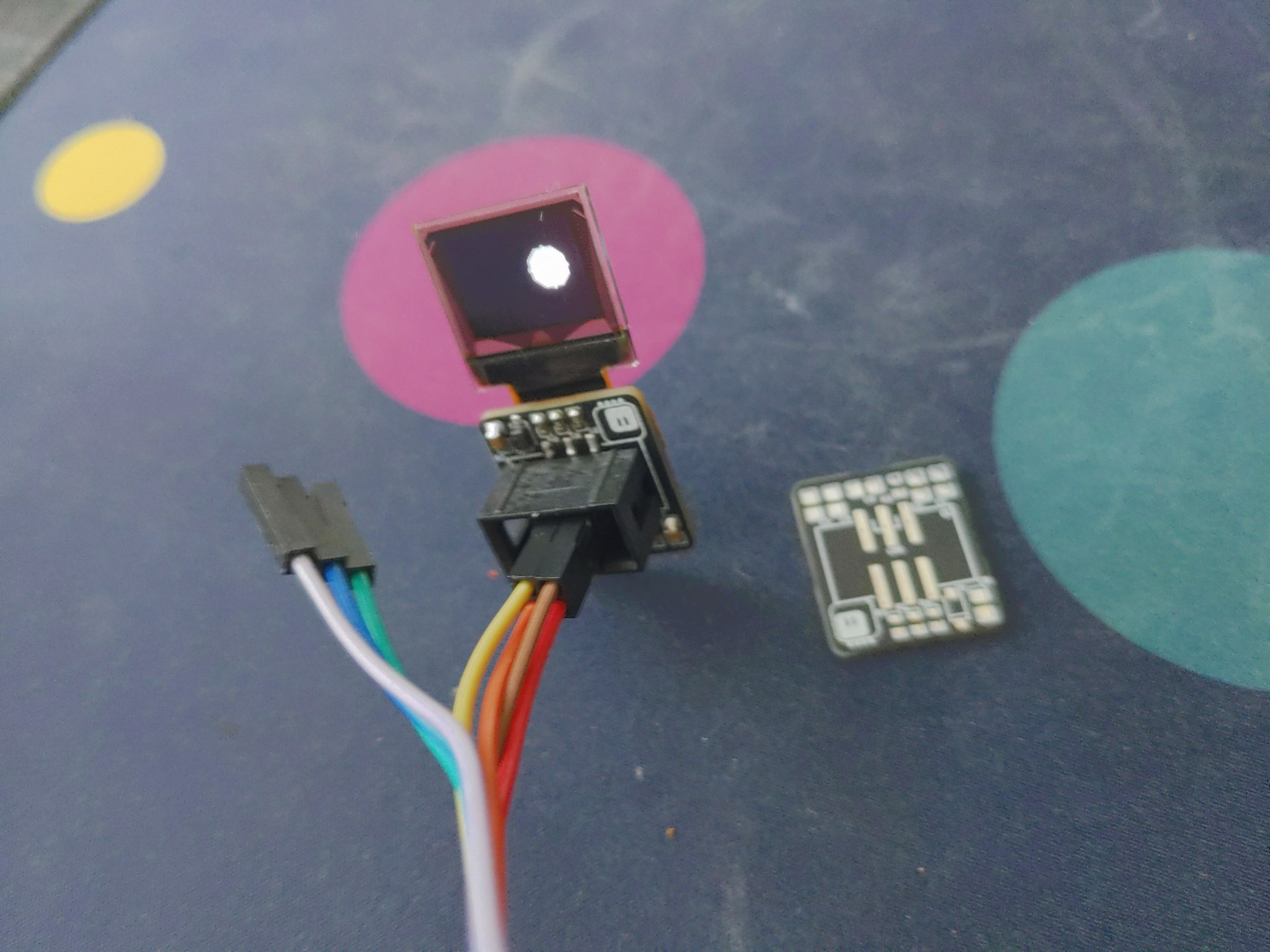
It all works. Only... Now that I tried to connect it to an actual badge, I noticed that... the first prototype was actually correct. The second one is mirrored. The specification for the SAO connector is showing a mirrored footprint, because of course KiCAD.
So the original designs were actually correct, and the new one is wrong. Great.
There is only one tiny problem. I didn't save the previous design. I was so sure it was wrong, I fixed it in place. And since I didn't want people to download the wrong files, I deleted the files I uploaded here. So now I have to re-fix the design.
Discussions
Become a Hackaday.io Member
Create an account to leave a comment. Already have an account? Log In.