 CriptasticHacker
The battery terminals slide in nicely (as do the batteries - it's a cool design) but no accomodation was made to keep the terminals at a safe distance from shorting. What's more, they have to have their solder tabs cut. Personally, I would have opted for a 2mm thicker pen:
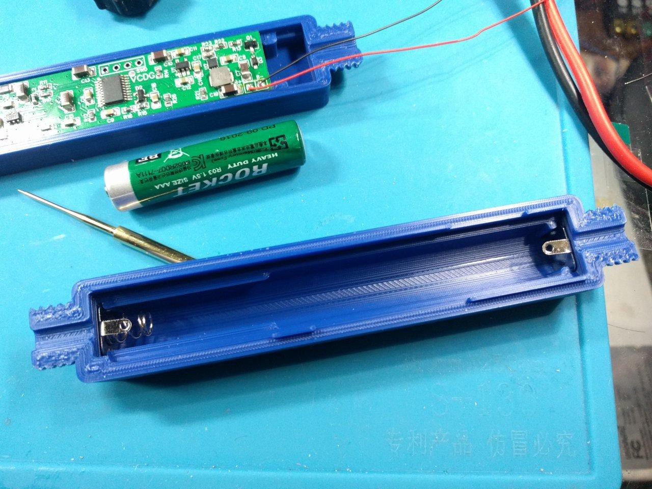
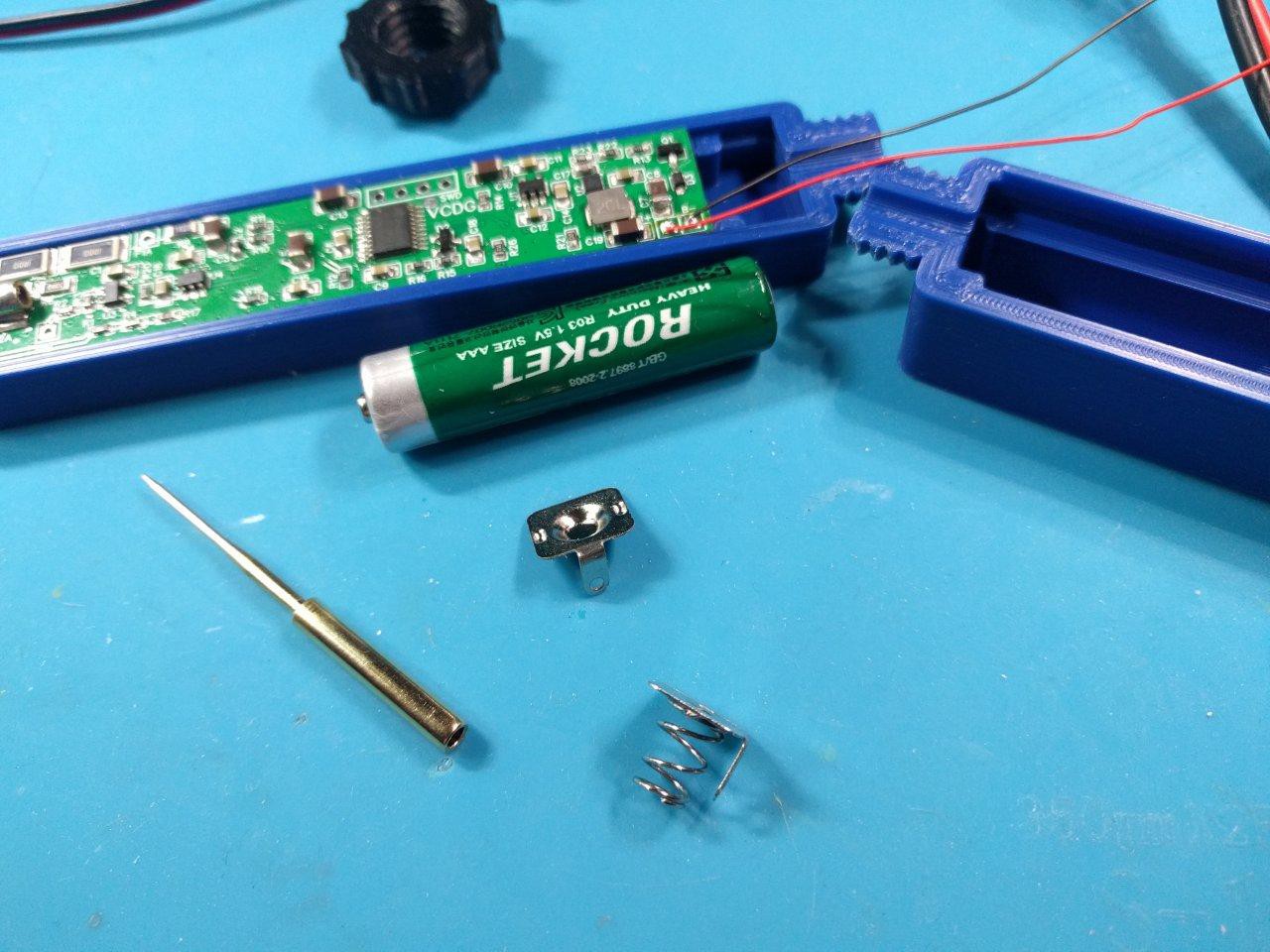
Again, I ended up using insulating polyimide over the contacts and under the main probe. Sadly, the positive terminal can short to the motherboard if you're not careful - it was not designed with any unpopulated courtyard on the PCB to avoid this, the way consumer products usually are.
After this, you'll need to connect 2 wires (ideally insulated together - like from an old audio cable) to PB1A and PB2A. these are the through hole solder joints under the display. This cable, or rather, those 2 conductors, travel through the 3D printed back nut and then get soldered to another externnal pinpoint probe. This is what completes the circuit - 2 wires (to their own test probe) and the built-in test probe So, a 3-wire Kelvin setup!
At the end of the day, it does come together and it does work. and it's free and open source!
Discussions
Become a Hackaday.io Member
Create an account to leave a comment. Already have an account? Log In.