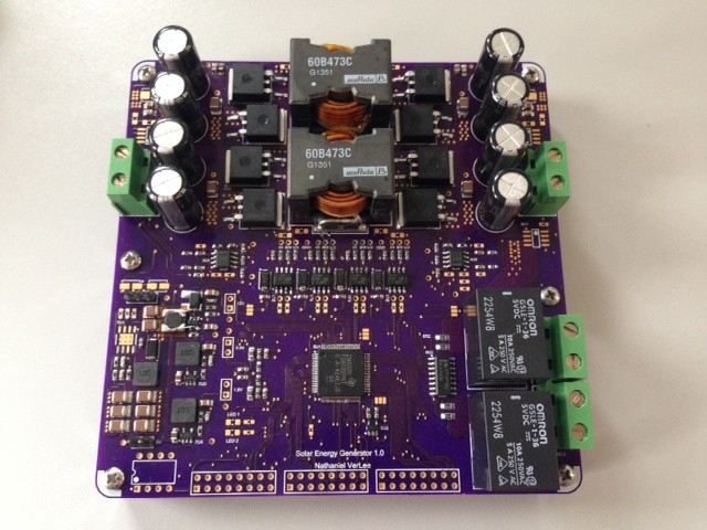
It has been awhile, but the boards came about two weeks ago and I started assembling them. Here is the first sone below. You can already see in the middle left area there is a silly mistake... oops. Kinda forgot that was a boost, not a buck, when I was doing the schematic capture. I havent found any show stoppers though. As I am in the middle of moving I have not had much time to start testing and validations of the circuits. As soon as I get my lab equipment set back up im hoping to do just that.
About time for an update... Board is here!
A project log for Solar Energy Generator
A solar energy system up to 500W in power for use with lithium batteries.
 Nathaniel VerLee
Discussions
Become a Hackaday.io Member
Create an account to leave a comment. Already have an account? Log In.